Ron Wilson, Altera
The power supply design of modern systems is a difficult task. This is not news. Demand for advanced chips continues to rise – huge bursts of current, decades of operating cycles, fast transients, and digital-mode control have transformed the point-of-load (PoL) supply from algorithmic practice to high-bandwidth mixed signals that are full of risks design. Conversely, the pressure to increase plant-level efficiency is pushing high DC voltages (48V and above) from the bottom of the rack or back of the chassis to the CPU and SoC. Distressed power designers must try to develop an excellent mixed-signal network.
Power supply side
The challenge first came from large DC regulators. In the field of aircraft, 28 V DC has already become a de facto standard. In the field of hybrid and electric vehicles, batteries may use hundreds of volts of direct current. Telecommunication or server racks can be assigned direct current from 12V to 48V.
In general, you need to reduce this high voltage when distributing power to a single board. However, if the system is large or efficiency is an important consideration, a multi-layer buck regulator may not be the best choice. According to efficiency, you need to use high DC voltage for the system as much as possible.
Some designers discuss the direct use of 48V voltage to power PoL regulators. In a recent demonstration, Google claims that its 48V rack architecture can reduce power distribution losses to 1/16th of a 12V rack. Google’s approach is to directly supply 48V power to PoL regulators to handle large loads such as CPUs or DRAM arrays, while reducing large voltages to 12V to meet the more complex requirements of specialized regulators.
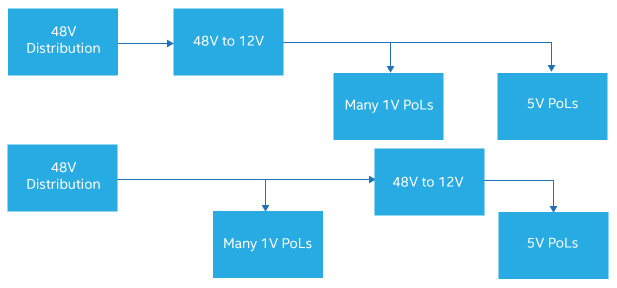
Figure 1. Some system designers provide 48V directly for PoL regulators in data centers and other similar large systems.
However, some people oppose this practice. The existing infrastructure of 12V systems is very large. They use chip MOSFET switches and commercial (or at least inexpensive) regulators. One thing is to be sure that single-stage 48V PoL regulation requires much higher GaN switching transistors. Mark Davidson, Intel PSG power manager, said: "In the final analysis, this is a matter of balancing capital expenditures and operating expenses. The 48V PoL can increase the efficiency of a truly large-scale deployment, but reducing the high voltage to 5-8V allows you to use lower cost PoL."
Low-voltage power distribution also allows you to use a wider range of PoLs with special functions. As the demand for system-on-chips becomes increasingly complex - CPUs, FPGAs, GPUs, and system-on-chips will consume a lot of power, this flexibility may eventually be essential.
Chip requirements
This section first discusses a purely physical phenomenon: the end of the threshold voltage adjustment. Below 90 nm, as the transistor size decreases, the fabrication designer begins to lose the ability to reduce the threshold voltage, parasitic capacitance, and interconnect series resistance. Enclosed Dennard Scaling supports avoiding optimal power density when the transistor is getting smaller. This means that in the near future, the chips we developed could be damaged at full speed.
As a result, modern power management strategies came into being. In the beginning, we only used the clock adjustment: if the chip starts to overheat or you don't need full speed performance, you can turn down the clock frequency. However, when static power consumption becomes as important as dynamic power consumption, designers need to reduce voltage and frequency. Therefore, implementing dynamic voltage frequency regulation (DVFS) and direct power gating is essential. By reducing the voltage, these technologies help designers control dynamic and static power consumption.
But there will always be one or two problems. In most systems, slowing down, especially shutting down function modules can cause a lot of delays, especially when they have a large number of internal states. The chip needs to monitor its expected workload to look for opportunities to save power, track the chip temperature, and understand the normal operation of self-protection. In general, the chip must also rely on external clues about the operation of the workload.
In addition, power management circuits must coordinate complex situations. For example, you may need to freeze the module, isolate it from the surrounding modules, save its state, change the supply voltage and frequency, wait for stable operation, reinitialize the module (if the module has stopped running, restore the state), and reconnect it To the system. All these operations can take a few milliseconds, so if you can't accurately determine how long the module will be needed again, it will increase power consumption and reduce system performance. Throughout the process, the voltage regulator and clock source must immediately respond to detailed commands from the power manager.
This dynamic situation is not the only complex problem that modern power supply networks face. There are also sorting issues. Obviously, different modules in the system-level chip will require different voltages at different times. The rate of increase and decrease in sequence and power supply, especially during power up and power down of the chip, is often critical to avoid interface lockup between modules and even physical damage to the circuit. Therefore, the PoL regulator must accurately and accurately respond to specific voltage adjustment commands.
Even without a request to change the voltage, the load changes drastically, placing additional burden on the PoL. Intel Circuit Researcher James Tschanz stated: "Powerful power gating can suddenly reduce the power consumption of rails from tens of watts to a few milliwatts." In modern CPUs or system chips, signals from the operating system and even command dispatch units may control Power consumption of large function modules such as vector processors or all CPU cores. Therefore, the PoL must track large current swings without voltage errors or breaking noise specifications. In some cases, the dynamic range of these loads may be higher than the regulator's effective range or even the entire certified operating range. Designers may need to dynamically switch between a buck regulator (which is usually more efficient at high currents) and a low noise low dropout (LDO) regulator (which is more efficient at low currents).
In addition, some of the loads on these large chips and on the motherboard around them have special requirements. Non-volatile memory chips may require higher voltage for programming. DRAM memory may have its own power management strategy and consume a lot of power. FPGAs can have high inrush currents and complex sequencing requirements. On large FPGAs, CPUs, and system-on-chips, analog circuits and SRAM modules may have unusually stringent noise requirements.
In addition, with the increasing use of PCI Express (PCIe), multi-gigabit Ethernet, and even faster serial links, transceivers have begun to become a category of circuits that have particularly high power supply noise requirements. Power supply noise specifications on high-speed serial transceivers typically exceed almost all switching regulators (except for several switching regulators), so power supply designers typically use linear PoL regulators on these specific rails.
The situation we described is not optimistic. When performing control, sequencing, and telemetry, the system-on-chip may be surrounded by a series of PoL devices: high-current, multi-mode, multi-voltage switching regulators, low-cost fixed-function transfer switches, high-efficiency or LDO regulators, and large regulators And microcontroller unit (MCU) or FPGA.
This problem is losing control. It requires too much information. For example, details about the transient requirements of some large chip DC rails may not be publicly released, and the transient response information of some regulators may not have been publicly released. This design will affect motherboard placement and routing in a very crowded space for large chips. Try to answer some seemingly simple questions, such as "When the CPU core switches from Turbo to Shutdown mode, will my 25G Ethernet channel keep running?" This requires mixed-signal simulations, and many design teams lack the corresponding Tools, models, and even expertise. From initial design to achieving on-site reliability goals, the relevant teams often deploy large-scale capacitors on a large scale.
Explore solutions
This issue is already very serious and different industry players are trying to solve: system-level chip designers, PoL regulator designers, and startups with new ideas. Everyone is working to ease the burden on the system design team.
In solving this problem, one of the most ambitious plans is to integrate all PoL into large chips. Tschanz talked about Intel's Fully Integrated Voltage Regulator (FIVR) program, which has deployed switches and linear regulators together on some CPUs. Tschanz explained: "With the inductors integrated into the package, we can place the switching regulators near the modules they supply. And we can place the LDOs on the die memory and near the PLL."
Intel's design work is of great importance, with multiple requirements, such as the use of high-voltage mixed-signal circuit designs in digital processes, integrating inductors into cost-constrained packages. But as a result, customers only need to provide relatively simple 1.8V rails without having to understand the power management of the chip.
Regulator manufacturers are participating. The new design includes a PoL with multiple output voltages and a digital interface that allows PoL and power controllers to communicate in both directions. Paying close attention to transient behaviors will help. At least one company is using a much higher than normal exchange frequency on its switching regulators to meet stringent noise immunity requirements.
Startup company AnDAPT has launched a more creative approach, and Intel has disclosed that it has invested in the method. Kapil Shankar, CEO of the company, said that when design issues start to present too much uncertainty, the industry will usually focus on improving programmability, blaming the problem on software or programmable logic.
Shankar said: "In this case, the MCU is not the ideal solution. Especially when implementing multiple concurrent real-time tasks, the MCU cannot guarantee the deterministic latency required for current power management." Sometimes, you need to change the analog path design, Instead of digital control functions, the software itself cannot help.
AnDAPT is unique in its approach to using a field-programmable, mixed-signal chip called an adaptive multi-rail power platform. If you already have some experience in the industry, you may first think of the emergence of programmable analog chip start-up companies, and their prospects are bright. However, the AnDAPT chip is undoubtedly a unique solution (Figure 2).
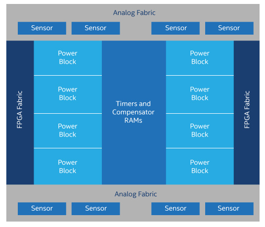
Figure 2. The AnDAPT power platform provides a set of building blocks to create a complete PoL solution.
The AnDAPT architecture does not use a unified array of analog elements (an intuitive, rich architecture that has not met practical application requirements for many years), but instead uses two SRAM programmable architectures (ie, analog and digital architectures). The former is basically a configurable architecture for analog signal paths, the latter being a conventional lookup table and register FPGA fabric. But the core of chip design is not the architecture, but a set of configurable dedicated modules, including: power module, sensor module, Compensator RAM and timer. AnDAPT does not require customers to build transistors, passives, gates, and register functions, but rather provides function templates to configure large modules that implement specific functions.
For example, some templates can configure the power module as any switching regulator, LDO regulator, current protection circuit, or current sense DAC/comparator. It also supports other functions. The sensor module can be an error digitizer, comparator, measurement amplifier, or reference DAC. Compensation RAM works with the algorithm functions in the FPGA fabric to use as a lookup table to implement transfer functions and support digital control loops. The FPGA fabric also implements a state machine to support control, sequencing, and interface functions. The analog architecture provides analog interconnects.
You can select, configure, and connect the required modules via the graphical user interface just as you would select a discrete graphics card from the catalog. Then you can design a device integration simulation tool for yourself.
Not all designs require AnDAPT-level flexibility, especially if CPUs, FPGAs, and system-on-chip vendors integrate power supplies into their packages. But during the transition period, system architects and design managers need to understand their choices—large-scale power distribution, large chips, and even memory and interconnect—that will create demand for the design team.
Product description:
Removable frying pot&basket with non-stick coating
Automatic shut-off with ready alert
304 stainless steel heating element
Heat resistant material inside enclosure
Removable and heat insulation handle for frying basket
Prevent slip feet
With fan guard,more safety
Certificates: GS CE CB SAA RoHS LFGB
Colour: customized
English manual&cookbook
5L Air Fryer,Air Fryer Deep,Hot Air Fryer,Industrial Deep Fryer
Ningbo Huayou Intelligent Technology Co. LTD , https://www.homeapplianceshuayou.com