Based on the detailed introduction of electromagnetic interference theory, the electromagnetic compatibility software and hardware design of the brushless DC motor control system is analyzed. The electromagnetic compatibility design is beneficial to improve the anti-interference ability of the brushless DC motor control system and enhance the system. Reliability and stability.
1 electromagnetic interferenceFamiliarity with and understanding of common sources of electromagnetic interference is one of the keys to discovering and solving electromagnetic interference problems. Electromagnetic interference can be divided into two categories: natural and artificial. The so-called natural refers to the electromagnetic interference phenomenon inherent in nature that is not related to human activities. The so-called man-made refers to electromagnetic interference caused by human industrial and social activities [1, 2].
1.1 Electromagnetic interference sourceSuch as lightning discharge phenomenon, motor TTL logic components, dynamic RAM, power supply, oscillator and transformers will produce high-frequency electromagnetic waves or noise during operation, seriously affecting the normal operation of the motor.
1.2 Coupling approach of electromagnetic interference energyCoupling refers to the connection of energy between circuits, devices, systems, and other circuits, devices, and systems. Various electromagnetic disturbance sources transmit electromagnetic energy to sensitive devices through coupling. There are two ways of coupling: conduction coupling and radiation coupling.
1.2.1 Conductive coupling
Conduction coupling is performed by connecting channels such as power lines, signal lines, interconnect lines, and ground conductors. According to the coupling method, it can be divided into three basic modes: common impedance coupling, capacitive coupling and inductive coupling. In practice, these three methods have a synergy at the same time.
1) Common impedance coupling
When the circuit current passes through a common impedance, the voltage developed by one circuit at that common impedance affects the other. The common power supply impedance coupling model and its equivalent circuit are as follows:
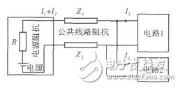
Figure 1 Common power supply impedance coupling model
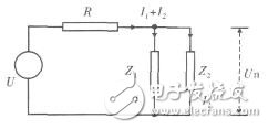
Figure 2 Common power supply impedance equivalent circuit
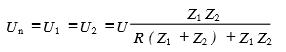
In FIG. 2, the power supply impedance and the common line impedance in FIG. 1 are combined and represented as R, U is an ideal voltage source, and Z1 and Z2 are impedances of circuit 1 and circuit 2, respectively. According to the equivalent circuit there are:
It can be seen from the above equation that any change in the supply current of the circuit 1 will affect the power supply voltage of the circuit 2 due to the presence of R. If R=0, then U1=U2=U, that is, circuit 1 and circuit 2 have no common impedance coupling. Reducing the common impedance coupling between circuit 1 and circuit 2 reduces the source impedance and the common line impedance. On the one hand, the power supply lead of the circuit can be close to the power output end, and the common line impedance can be reduced by reducing the length of the power line; on the other hand, the power supply can be used to reduce the internal resistance of the power supply [3].
2) Capacitive coupling
Capacitive coupling is caused by the electric field interaction between two circuits. The coupling model and equivalent circuit are as follows:
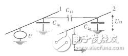
Figure 3 Capacitive coupling model
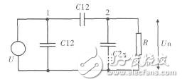
Figure 4 Capacitive coupling equivalent circuit
C12 is the distributed capacitance between conductor 1 and conductor 2, C1g is the capacitance between conductor 1 and ground, C2g is the capacitance between conductor 2 and ground, R is the resistance between conductor 2 and ground, U1 is used as disturbance The voltage of the conductor 1 of the source, the circuit 2 is the disturbed circuit, and Un is the disturbance voltage generated between the line 2 and the ground.
According to the equivalent circuit, there are:
If R is low impedance and is satisfied  then
then
![]() (1)
(1)
If R is high impedance and is satisfied ![]() then
then
![]() (2)
(2)
Equation (1) shows that the capacitive coupling disturbance is equivalent to a current source with an amplitude of In=jwC12U indirectly between conductor 2 and ground. In the case where the source voltage and frequency of the disturbance source are constant, the coupling interference is reduced. On the one hand, the sensitive circuit can be operated at a lower resistance value, that is, the Un is reduced by reducing the R; on the other hand, the conductor is appropriately passed. Orientation, shielding, or isolation reduces C12 to achieve a reduction of Un.
Equation (2) shows that the capacitive coupling disturbance is only related to C12 and C2g in the case of high impedance, and the disturbance generated at this time is much larger.
3) Inductive coupling
Inductive coupling is caused by the interaction of the magnetic fields between the two circuits. The coupling model and equivalent circuit are as follows:

Figure 5 Inductive coupling model
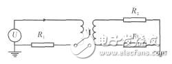
Figure 6 Inductive Coupling Equivalent Circuit
The disturbance voltages generated by the interference power source I1 in the circuit 1 on the load resistors R and R2 of the circuit 2 are:
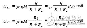
Where S is the loop area and B is the effective value of the sinusoidal flux density of the angular frequency. It can be seen from the above formula that the purpose of inductive coupling disturbance can be reduced by reducing B, S, and cos θ.
1.2.2 Radiation coupling
Radiation coupling is the transmission of electromagnetic energy from a source of disturbance to a sensitive device in the form of an electromagnetic field. In addition to the intentional radiation of the disturbance source, there are many electromagnetic waves that are unintentionally radiated, and the conductors in this electromagnetic field can induce voltage. Therefore, radiation interference can be achieved by means of antennas, wires, closed loops, etc.
The motor control system interferes.
2 Electromagnetic compatibility design of system hardwareThe DSP circuit has a high operating frequency and the chip pins are very dense. When designing a digital-analog hybrid with an analog device, the design of the PCB version is very high [4]. The following are guidelines and requirements that must be followed when designing.
With the miniaturization and packaging of electronic devices, it is necessary to use multilayer printed circuit boards, including separate digital ground planes, power planes and other signal layers. In the wiring, a separate power supply layer is beneficial to the layout of the circuit board components; the use of the ground layer not only saves a lot of device pin grounding workload, but also can effectively improve the quality of the digital ground wire. However, it should be noted that the through-hole pads and vias should be interrupted during the routing and routing. Excessive vias will affect the anti-interference effect of the formation. The system adopts a four-layer board structure, which is a ground layer, a power layer and a two-layer component layer. The use of via pads and vias is also specifically considered in drawing PCBs, and as many networks as possible are routed through the component layers.
Since the DSP core-based motor control system uses a separate power supply mode, more power solutions are required for the TSM320LF2407A with 144 pins.
Coupling capacitors, in order to save space and reduce the number of through holes, the system uses chip capacitors, achieving a good decoupling effect.
The basic principle that grounding should follow is that the digital ground, analog ground, and shield ground should be properly grounded and cannot be mixed. As far as possible, the ground circuits are each formed into a loop, reducing the current coupling between the circuit and the ground. Reasonably arranging the ground wire limits the current to as small a range as possible, and designs the printed circuit and grounding method of the corresponding width according to the magnitude and frequency of the ground current. The A/D sampling analog power supply pins VCCA and VSSA of the DSP must be distinguished from any digital voltage supply pins to avoid digital interference signals being coupled through the ground. At the same time, the analog ground of the A/D converter uses a single point of contact, digitally connected to the analog ground at the power source and connected to the ground here. VCCA and VSSA analog leads should be routed as short as possible on the printed circuit board to match the two correctly.
3 software electromagnetic compatibility designThe TSM320LF2407A has a rich instruction set, extremely high operating speed, and software watchdog and real-time interrupt (RTI) modules, all of which provide good conditions for software anti-jamming. This system mainly uses the following software anti-interference design.
3.1 software trap methodDue to interference, it often causes the running program to enter the blank area of ​​the program memory (ie, no instruction area). This phenomenon is called the program "running away". Therefore, three sub-operations (nop) are written between each subroutine, between each function module and all blank spaces, followed by an unconditional branch instruction. Once the program flies to these areas, it will automatically return to execution. Normal procedure. which is:
Nop
Nop
Nop
LJMPADDRESS: ADDRESS specified address;
3.2 Program redundancy designIn the blank area of ​​the program memory, some important data tables and programs are written as backups, so that the backup parameters and programs keep the system working properly when the system is destroyed. Since the data storage of the LF2407A is based on the data page, if the data of different data pages is operated without specifying the corresponding data page, the program will run away. Therefore, it is necessary to fill the data pages that are not used by the program to prevent the data page from being confusing and causing the system to malfunction.
3.3 Software Watchdog DesignThe Watchdog Timer (WDT), also known as the Watchdog Timer, allows the microcomputer system to recover from a fault. The WDT is also started when the microcomputer system starts up. It will count the state cycle of the machine, and each state cycle counter will increment by one. When the counter overflows, it can automatically lower the level of the reset pin for at least two state cycles. This reset signal causes the DSP to reset. During normal operation, the software is used to periodically reset the WDT without causing a WDT overflow to cause a system reset. However, if the program "runs away" into an infinite loop or a misunderstanding, then the software will not reset the WDT, causing the WDT count to overflow and reset the system. After the system is reset, the program is executed from the 000H unit, so that the "running" program can be pulled back to the normal program.
4 ConclusionElectromagnetic compatibility design is related to the safe operation of DSP-based motor control systems. The design of the motor control system should be based on the working environment of the system, the technical indicators of the control system, process complexity, cost and other factors for the comprehensive design of electromagnetic compatibility. The design of the motor control system adopts the above electromagnetic compatibility design, which makes the operation stable and reliable, and the failure rate is low, achieving the expected effect!
Compact Solar Water Heating System
Different from split Solar Water Heating System, compact solar water heating system mainly means the system with Vacuum Tubes or heat pipe vacuum tubes inserting into water tanks directly. Compact solar water heating system can be both non-pressurized and Pressurized Solar Water Heating System, it defines solar water heating system only by system structure.
Compact system mainly means the household solar water heating system.

Solar Heating System,Compact Hot Water System,Compact Water Heating System,Compact Solar Water Heating System
Linuo Ritter International Co.,Ltd , https://www.lnrtsolarenergy.com