The three converters shown in the figure below work by storing energy and then releasing the energy in a controlled manner to get the desired output voltage. For a job, the best switching DC/DC converter can meet the overall needs of the system with minimal installation costs. This can be measured by a set of parameters describing the performance of the switched DC/DC converter, including: high efficiency, small mounting size, small quiescent current, low operating voltage, low noise, high functional integration, enough Output voltage regulation capability, low installation cost.
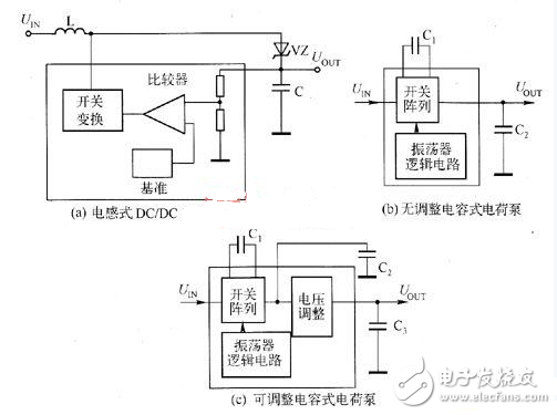
Three typical DC/DC converter block diagrams
Work efficiency
1 Inductive DC/DC converter: The conversion efficiency of the battery-powered inductive DC/DC converter is 80%-85%, and the loss mainly comes from the external diode and the modulator switch.
2 Voltage-free charge pump: a basic charge pump (such as TC7660H). It has a very high power conversion efficiency (generally over 90%) because the loss of the charge pump is mainly from the ESR of the capacitor and the on-resistance (RDS-ON) of the internal switching transistor, both of which can be done very well. low.
3 Charge Pump with Voltage Regulation: It is a linear regulator that adds a low dropout voltage after the output of the basic charge pump. Although voltage regulation is provided, its efficiency is degraded due to the power consumption of the back-end regulator. For maximum efficiency, the output voltage of the charge pump should be as close as possible to the regulated voltage of the back-end regulator.
The best choices in design applications are: voltage-free charge pumps (in applications that do not require stringent output regulation), or voltage-regulated charge pumps (if the differential pressure across the back-end regulator is small enough).
Installation size
1 Inductive DC/DC Converters: Although many new inductive DC/DC converters are available in SOT packages, they often still require external inductors with large physical shapes. Moreover, the circuit layout of the inductive DC/DC converter itself requires a large board space (additional decoupling, special ground processing, shielding, etc.).
2 Voltage-free charge pump: The charge pump does not use an inductor, but requires an external capacitor. The new charge pump device is packaged in a SOP and operates at a higher frequency, so a small capacitor (1μF) with a small footprint can be used. The space occupied by the charge pump IC chip and the external capacitor is not as large as the inductance in the inductive DC/DC converter. It is also easy to obtain positive and negative combinations of output voltages using a charge pump. For example, the TCM680 device can support +2 UIN output voltage with only external capacitors. Inductive DC/DC converters require two independent converters to achieve the same output voltage. For example, with a converter, a transformer with a complex topology is required.
3 Charge Pumps with Voltage Regulation: Adding a discrete back-end voltage regulator takes up more space, however many of these regulators have SOT-style packages that reduce the footprint. New voltage-regulated charge pump devices, such as the TCM850, integrate a charge pump, back-end voltage regulator, and shutdown control in a single 8-pin 50lC package.
The best choice in design applications is: no voltage regulation or a voltage regulated charge pump.
Quiescent Current
1 Inductive DC/DC converter: Frequency modulation (PFM) Inductive DC/DC converter is a switching DC/DC converter with minimum quiescent current. Voltage regulation by frequency modulation can minimize supply current under small load current. .
2 Voltage-free charge pump: The quiescent current of the charge pump is proportional to the operating frequency. Most new charge pumps operate at frequencies above 150 kHz, allowing the use of capacitors of 1 μF or less. To overcome the large quiescent current problem, some charge pumps have a shutdown input pin to turn off the charge pump for long periods of time, thereby reducing the supply current to near zero.
3 Charge pump with voltage regulation: The back-end voltage regulator increases the quiescent current, so the charge pump with voltage regulation is worse than the basic charge pump in terms of quiescent current.
The best choice in design applications is: inductive DC/DC converters, especially frequency modulation (PFM) switching.
Minimum working voltage
1 Inductive DC/DC Converter: Battery-powered inductive DC/DC converters (such as TC16) can be started up to as low as 1V or less, making them ideal for single-cell battery powered electronics.
2 Voltage-free charge pump / voltage-regulated charge pump: Most charge pumps have a minimum operating voltage of 1.5V or higher, making them suitable for applications with at least two batteries.
The best choice in design applications is: inductive DC/DC converters.
Generated noise
Inductive DC/DC Converters: Inductive DC/DC converters are a source of power supply noise and switching radiated noise (EMI). Broadband PFM inductive DC/DC converters generate noise over a wide frequency band. It is possible to increase the operating frequency of the inductive DC/DC converter so that the noise generated falls outside the frequency band of the system.
2 Voltage-free charge pump / charge pump with voltage regulation: The charge pump does not use an inductor, so its EMI effect can be ignored. Pump input noise can be eliminated with a small capacitor.
The best choice in design applications is: no voltage regulation or charge pump with voltage regulation.
Integration
1 Inductive DC/DC Converters: Chips with integrated switching regulators and other functions such as voltage detectors and line conditioners have been developed. For example, the TC16 chip integrates a PFM boost converter, LD0 and voltage detector in a SO-8 package. These devices offer superior electrical performance and take up less space than discrete implementations.
2 Voltage-free charge pump: Basic charge pump, such as TC7660, has no additional function integration and takes up little space.
3 Charge Pump with Voltage Regulation: Integrating more functions with voltage-regulated charge pump chips has become a current trend. It is clear that the functional integration of the next generation of regulated charge pumps will be comparable to that of inductive DC/DC converter integrated chips.
The best choice in design applications is: inductive DC/DC converters.
Output adjustment
1 Inductive DC/DC converter: Inductive DC/DC converter has good output regulation capability. Some inductive DC/DC converters also feature external compensation pins that allow for “fine tuning†of the transient response characteristics of the output.
2 Voltage-free charge pumps: These devices have no voltage regulation at their output. They simply convert the input voltage to a negative or multiple of the output voltage. In this case, the output voltage will decrease as the load current increases. While this is not a problem for some applications, such as LCD biasing, it is not suitable for applications that require a stable output voltage.
3 Charge-regulated charge pump: It provides voltage regulation (regulation) through the back-end linear voltage regulator (on-chip or external). In some cases, it is necessary to increase the number of switching stages for the charge pump to provide sufficient headroom for the back-end regulator, which requires an increase in external capacitance, which can have a negative impact on size, cost, and efficiency. However, the back-end linear regulator allows the output voltage of the regulated charge pump to be as stable as an inductive DC/DC converter.
The best choice in design applications is a charge pump with voltage regulation.
Installation cost
1 Inductive DC/DC converter: In recent years, the cost of using an inductive DC/DC converter has gradually decreased, and the demand for external components has also become less. However, an inductive DC/DC converter requires at least one external inductor, capacitor, and Schottky diode. Diodes, inductors, and relatively high-priced switching converter chips have higher total cost than charge pumps.
2 Voltage-free charge pump: A voltage-free charge pump is less expensive than an inductive DC/DC converter and requires only external capacitors (no inductor), saving board space, inductor cost, and shielding in some cases. cost.
3 Charge Pump with Voltage Regulation: The cost of a charge pump with voltage regulation is approximately equivalent to the cost of an inductively switched DC/DC converter. In some cases, an external back-end voltage regulator can be used to reduce cost, but it increases the required installation space and reduces work efficiency.
The best choice in design applications is: in the case where strict regulation is not required, the best choice is a voltage-free charge pump; if it is required for output voltage regulation, select a charge pump and inductor with voltage regulation. The cost of a DC/DC converter is roughly equivalent.
1. The connection is convenient and flexible. 2. Small volume. 3. A kinds of channel choice. 4. cooperate with prefabricated cable connection.
The Relay Module integrates and serializes the single small power library relay in the electrical control cabinet, reduces the intermediate wiring link and improves the product performance. The product conforms to the development trend of miniaturization and integration, and is the renewal product of the original single relay. The installation form adopts the general 35mm U-shaped guide rail for installation, which is convenient and fast.Our products are made of Idec, Omron, Tyco, Panasonic relay and deca terminal.
Breakout Board,Breakout Module,CNC Breakout Board,USB Breakout Board
Suzhou WeBest Electronics Technology Co.Ltd , https://www.webestet.com