This article focuses on three IGBT drive circuits. The function of the driving circuit is to power the pulse outputted by the single chip to drive the IGBT to ensure the reliable operation of the IGBT. The driving circuit plays a vital role. The basic requirements for the IGBT driving circuit are as follows:
(1) Provide appropriate forward and reverse output voltages to reliably turn the IGBT on and off.
(2) Provide sufficient transient power or instantaneous current to enable the IGBT to quickly establish a gate-controlled electric field to conduct.
(3) The input and output delay time is as small as possible to improve work efficiency.
(4) High enough input and output electrical isolation to insulate the signal circuit from the gate drive circuit.
(5) Sensitive overcurrent protection.
Drive circuit EXB841/840
The working principle of EXB841 is shown in Fig. 1. When the current of 10 mA of the 14-pin and 15-pin of EXB841 flows through 1us, the IGBT is normally turned on, VCE drops to about 3V, and the voltage of 6-pin is clamped at about 8V. Since the VS1 regulation value is 13V, Therefore, it will not be broken down, V3 will not conduct, the potential of point E is about 20V, and the diode VD is cut off, which does not affect the normal operation of V4 and V5.
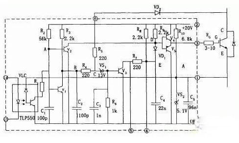
When there is no current flowing through pins 14 and 15, V1 and V2 are turned on, V2 is turned on to make V4 turn off, V5 is turned on, IGBT gate charge is rapidly discharged through V5, and pin 3 potential drops to 0V, which is IGBT gate. The negative IGBT with a negative bias of about 5V is used, and the IGBT is reliably turned off, and the rapid rise of VCE causes the pin 6 to "float". The discharge of C2 makes the potential of point B 0V, then V S1 is still not conducting, the subsequent circuit does not operate, and the IGBT is normally turned off.
If an overcurrent occurs, the V CE of the IGBT is too large to make VD2 cut off, so that VS1 breaks down, V3 turns on, C4 discharges through R7, and the potential at point D drops, so that the voltage UGE between the gates of the IGBT is lowered, and the completion is slow. Turn off to achieve protection of the IGBT. The process of overcurrent protection realized by EXB841 shows that the main basis for the EXB841 to determine the overcurrent is the voltage of the 6-pin. The voltage of the 6-pin is not only related to VCE, but also related to the turn-on voltage Vd of the diode VD2.
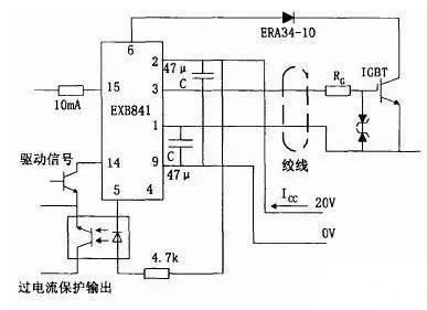
The typical wiring method is shown in Figure 2. Note the following points when using:
a, IGBT grid-emitter drive circuit round-trip wiring can not be too long (generally should be less than 1m), and should be twisted pair connection to prevent interference.
b. Since the IGBT collector generates a large voltage spike, increasing the IGBT gate series resistance RG is beneficial to its safe operation. However, the gate resistance RG cannot be too large or too small. If the RG is increased, the turn-on and turn-off time is prolonged, so that the turn-on power consumption is increased. Conversely, if the RG is too small, the di/dt is increased, and mis-conduction is likely to occur.
c. Capacitor C is used to absorb the change of supply voltage caused by the impedance of the power supply connection. It is not the power supply filter capacitor of the power supply. The value is generally 47 F.
d, 6 feet over current protection sampling signal connection terminal, connected to the IGBT collector through a fast recovery diode.
e, 14, 15 connected to the drive signal, generally 14 feet connected to the pulse forming part of the ground, 15 feet connected to the positive end of the input signal, the input current of the 15 end should generally be less than 20mA, so add a current limiting resistor before the 15 feet.
f. In order to ensure reliable turn-off and turn-on, a Zener diode is added to the gate emitter.
M57959L/M57962L thick film drive circuit
M57959L/M57962L thick film driver circuit is powered by dual power supply (+15V, -10V), output negative bias is -10V, input and output level is compatible with TTL level, with short circuit / overload protection and closed short circuit protection. It also has time delay protection. They are suitable for driving IGBTs of 1200V/100A, 600V/200A and 1200V/400A, 600V/600A and below. The M57959L/M57962L is excellent in driving effect and performance when driving medium and small power IGBTs, but when it works At high frequencies, the front and rear edges of the pulse become poorer, that is, the maximum transmission width of the signal is limited. And the inside of the thick film adopts the printed circuit board design, the heat dissipation is not very good, and the internal device is easily burnt due to overheating.
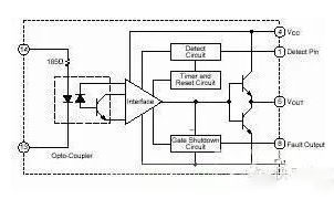
Japan's Mitsubishi's M57959L integrated IGBT dedicated driver chip can be used as 600V/200A or 1200V/100A IGBT driver. Its maximum frequency is also 40KHz, with dual power supply (+15V and -15V) output current peak value of ± 2A, M57959L has the following characteristics:
(1) Optocoupler is used to realize electrical isolation. The optocoupler is fast type, suitable for high frequency switch operation of about 20KHz. The primary side of the optocoupler has a series current limiting resistor, and the 5V voltage can be directly applied to the input side.
(2) If dual power supply driving technology is used, the output negative gate voltage is relatively high, and the limit value of the power supply voltage is +18V/-15V, which is generally +15V/-10V.
(3) The signal transmission delay time is short, the low-high transmission delay and the high-low transmission delay time are below 1.5μs.
(4) With overcurrent protection. M57962L determines whether the IGBT is over-current by detecting the saturation voltage drop of the IGBT. Once overcurrent, the M57962L will soft-shut down the IGBT and output an over-current fault signal.
(5) The internal structure of the M57959 is shown in the figure. The driving part of this circuit is similar to the EXB series, but the overcurrent protection is different. The overcurrent detection still uses voltage sampling, and the circuit features a gate voltage ramp-down to achieve IGBT soft turn-off.
Overvoltage and high current surges during turn-off are avoided. In addition, during the turn-off process, the state of the input control signal is disabled, and the protection shutdown is done in a closed state. When protection begins, a fault signal is sent immediately, with the goal of cutting off the control signal, including other active components in the circuit.
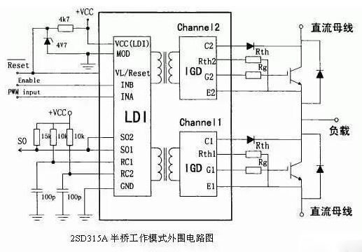
SD315A integrated drive module
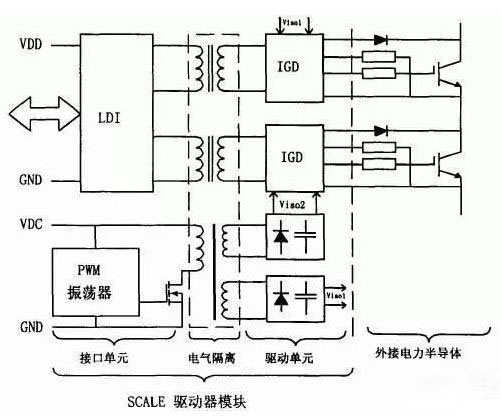
The integrated driver module is powered by a single +15V supply and integrates an overcurrent protection circuit. The biggest feature is safety, intelligence and ease of use. The 2SD315A can output large peak currents (maximum instantaneous output current up to ±15A), with high drive capability and high isolation voltage capability (4000V). The 2SD315A has two drive output channels suitable for driving two single-tube or one half-bridge dual-unit high-power IGBT modules with a rating of 1200V/1700V or more. When used as a half-bridge driver, it is convenient to set the dead time.
There are three main functional modules in the 2SD315A, which are LDI (Logic To Driver Interface), IGD (Intelligent Gate Driver), and DC/DC converters with input and output isolation. When the PWM signal is externally input, it is encoded by LDI. To ensure that the signal is not interfered by external conditions, the processed signal needs to be electrically isolated by a high-frequency isolation transformer before entering the IGD. The signal received from the other side of the isolation transformer is first decoded in the IGD unit and the decoded PWM signal is amplified (±15V/±15A) to drive the external high power IGBT. When the overcurrent and short circuit protection circuits in the intelligent gate drive unit IGD detect overcurrent and short circuit faults of the IGBT, the corresponding response time and blocking time are generated by the lockout time logic circuit and the state confirmation circuit, and the state at this time is obtained. The signal is encoded and sent to the logic control unit LDI. The LDI unit decodes the transmitted IGBT operating state signal and processes it in the control loop. In order to prevent the two output drive signals of the 2SD315A from interfering with each other, the DC/DC converter provides power supply that is isolated from each other.
Note when using 2SD315 :
a, working mode
The mode selection terminal MOD of the drive module is externally connected to the +15V power supply, and the input pins RC1 and RC2 are grounded for direct operation mode. The logic control level is +15V, and the signal input pins InA and InB are connected together to receive the pulse signal from the MCU. 2SD315A SO1 and SO2 two pin output channel working state. When MOD is grounded, MOD is grounded. Usually, the half-bridge mode is to drive one bridge arm on a DC bus. In order to avoid the straight-through of the upper and lower arms, the dead time must be set. In the dead time, both pipes are turned off at the same time. Therefore, the RC 1 and RC2 terminals must generate an dead time according to the requirements of an external RC network. The dead time can generally range from 100n to several ms. The RC 1 and RC2 shown in the figure are connected to the resistance of 10 k. and the capacitance of 100 pF, respectively, so that the dead time generated is about 500 ns.
b, port VL / Reset
This terminal is used to define the input InA and InB with the dense characteristic, so that the input is turned on at 2/3 VL and turned off at I/3 VL. When the PWM signal is TTL level, the terminal is connected as shown in Figure 3-5. When the input InA and InB signals are 15V, the terminal should be connected to the ++15V power supply through a resistor of about 1K. The turn-off voltage should be lov and 5V, respectively. In addition, there is another function in the input UL/Reset terminal: if it is grounded, the error message in the logic drive interface unit 1.DI001 is cleared.
c, gate output
The gate output Gx terminal is connected to the gate of the power semiconductor. When the SCALE driver is powered by 15V, the gate output is 15V. The negative gate voltage is generated internally by the driver. Using the circuit of the structure shown in Figure 3-6 can achieve different speeds of turn-on and turn-off, increasing the flexibility of user use.
d, layout and wiring
The driver should be placed as close as possible to the power semiconductor so that the leads from the driver to the power transistor are as short as possible. Generally, the driver should not be as long as 10 cm longer. At the same time, it is generally required to use a stranded wire for the collector and emitter leads, and an aligning Zener diode (15~18V) can be connected between the gate and the emitter of the IGBT to protect the IGBT from breakdown.
The mode selection terminal MOD of the drive module is externally connected to the +15V power supply, and the input pins RC1 and RC2 are grounded for direct operation mode. The logic control level adopts +15V, and the signal input pins InA and InB are connected together to receive the pulse signal from the single chip microcomputer for synchronous control. 2SD315A SO1 and SO2 two-pin external triode and optocoupler are used to output the working state of two output channels to the single-chip microcomputer. The output structure is open-collector output, which can be applied to various level logic through external pull-up resistor. . A light-emitting diode is placed between pins SO1, SO2 and the power supply and between VisoX and LSX for fault indication. Under normal conditions, both SO1 and SO2 outputs are high. After power-on, D3 and D4 are on first, and after a few seconds, they are off, and D8 and D15 are on.
When a fault signal is detected, the output levels of SO1 and SO2 are pulled down to ground, ie D3 and D4 are lit, while D8 and D15 are flashing. 2SD315A judges whether the loop is short-circuited or over-current by monitoring UCE(sat). When one-way or two-way over-current phenomenon is detected, the detection circuit will return the abnormal state to the drive module, and a fault signal will be generated inside the drive module. It is latched and the latch time is 1 s. During this time, the driver module no longer outputs a signal, but the two sets of IGBTs are turned off in time to protect them. At the same time, the high level of the state output pins SO1 and SO2 is pulled low, the optocoupler TLP521 is turned on, and the two state signals are sent to the single chip through the OR gate 74LS32. In order to prevent a high back electromotive force on the collector of the IGBT due to the shutdown speed being too fast, the circuit structure shown in the figure is used to achieve the difference in turn-on and turn-off speeds. The gate resistance is 3.4Ω at turn-on and 6.8Ω at turn-off. The diode is fast recovery, which reduces the turn-off speed to a safe level.
IGBT short circuit failure mechanism
Several consequences of IGBT load short circuit
(1) Exceeding the thermal limit: The intrinsic temperature limit of the semiconductor is 250 °C. When the junction temperature exceeds the intrinsic temperature, the device will lose its blocking ability. When the IGBT load is short-circuited, the junction temperature rises due to the short-circuit current. At the limit, the gate level protection also fails.
(2) Current holding effect: Under the normal working current, the IGBT has a small sheet resistance Rs and no current holding phenomenon, but in the short circuit state, the voltage drop on Rs is higher than 0.7V due to the large short circuit current. When J1 is positively biased, current is generated, and the gate level loses voltage control.
(3) Shutdown overvoltage: In order to suppress the short-circuit current, when the fault occurs, the control circuit immediately removes the positive gate voltage, turns off the IGBT, and the short-circuit current decreases accordingly. Due to the large short-circuit current, the current drop rate during turn-off is high, and a high voltage is induced in the wiring inductance, especially in the case where the induced voltage on the package lead inductance is hard to suppress, it will make the device An overcurrent has become a shutdown overvoltage and has failed.
IGBT overcurrent protection method
(1) Decompression method: refers to lowering the gate voltage when a fault occurs. Since the short-circuit current ratio is proportional to the plus-gate voltage Ug1, the positive-gate voltage can be lowered in the event of a fault.
(2) Method of cutting off the pulse: Since the Uce voltage rises during overcurrent, we use the method of detecting the collector voltage to judge whether the current is overcurrent, and if it is overcurrent, the trigger pulse is cut off. At the same time, the soft turn-off mode is adopted as much as possible to alleviate the drop rate of the short-circuit current and avoid the damage caused by the overvoltage.
Micro-probe type NTC mini Temperature Sensor with the properties of sensitiveness and fast response, has been used to rice cooker, electric heater and more others. Temperature range can be from -30°C to 200°C.
Feyvan Electronics designs and manufactures NTC temperature sensors, probes, and cable assemblies for more than 15 years experiences. With excellent long-term stability, high accuracy and short response time properties in high-temperature sensing applications such as automotive, home appliance and industrial use from -40℃ to +250℃, Feyvan electronics provide various choices for a wide range of applications and are available in custom engineered probe package configurations for a variety of mounting and connectivity options with low costs.
Mirco-probe Sensor
Micro-Probe Sensor,Small Temperature Probe,Temperature Sensor,Miniature Sensor
Feyvan Electronics Technology Co., Ltd. , http://www.fv-cable-assembly.com