Tags: LDO PCB
This article refers to the address: http://
As portable products become smaller and lighter, higher requirements are placed on power management chips, such as high integration, high reliability, low noise, anti-interference, and low power consumption. This article explores various aspects of the practical application of portable product power supply design.
The power supply design of portable products requires system-level thinking. When developing battery-powered low-power products such as mobile phones, MP3, PDA, PMP, DSC, etc., if the power system design is unreasonable, it will affect the architecture of the whole system and the characteristics of the product. Combination, component selection, software design, and power distribution architecture. Similarly, in the system design, we must also consider from the perspective of saving battery energy. For example, today's portable product processors typically have several different operating states, and the battery capacity can be reduced through a range of different power saving modes (idle, sleep, deep sleep, etc.). When the user's system does not require maximum processing power, the processor enters a low power mode with less power consumption.
From the development trend of portable product power management, the following issues need to be considered: 1. Power supply design must be considered from the overall system design such as cost, performance and time to market; 2. Portable products are becoming smaller and lighter, must be considered The power system is small in size and light in weight; 3. The power management chip is selected to strive for high integration, high reliability, low noise, anti-interference, low power consumption, break through the heat bottleneck and extend battery life; 4. Select new technology The design of the new power chip is the basic condition for ensuring the advanced nature of the product, and it is also the eternal pursuit of power management for portable products.
Common power management chips for portable products include: low dropout regulator (LDO), very low dropout regulator (VLDO), inductor-based energy storage DC/DC converter (buck circuit Buck, boost circuit Boost, drop) Buck-Boost, a charge pump based on capacitor energy storage, a battery charge management chip, and a lithium battery protection IC.
When selecting the power management chip, you should pay attention to: select the manufacturer with mature production technology and excellent quality; select the chip with high working frequency to reduce the application cost of the peripheral circuit; select the small chip to meet the volume requirement of the portable product; Choose a technology to support a good manufacturer, to easily solve problems in the application design; select a complete product data, samples and DEMO easy to apply, can supply a large number of chips; select a cost-effective chip.
The LDO linear low dropout regulator is the simplest linear regulator that can only reduce the input voltage to a lower voltage due to its inherent DC switching-free voltage conversion. Its biggest drawback is in thermal management because its conversion efficiency is approximately equal to the output voltage divided by the value of the input voltage.
The LDO current main channel is composed of a MOSFET plus an overcurrent detection resistor. The Schottky diode is used for reverse phase protection. The voltage divider resistor at the output is taken out to feed back the current of the MOSFET. The EN enable terminal can be used. From the outside to control its working state, internal over-current protection, over-temperature protection, signal amplification, Power-OK, reference source and other circuits are also set up. In fact, LDO is already a multi-circuit integrated SoC. LDO's ESD>4KV, HBM ESD>8KV.
The application of the low-dropout regulator is as simple and convenient as the three-terminal regulator. Generally, a filter capacitor can be added to the input and output terminals. The material of the capacitor has a significant effect on the filtering effect. It is necessary to use a low ESR X7R & X5R ceramic capacitor.
The main point of LDO wiring design is to consider how to reduce the noise and ripple on the PCB. How to take the line is a skill and experience, and it is also one of the keys to the success of the design. Figure 1 illustrates how to design a trace circuit diagram, master the nodes of current reflow, and effectively control and reduce noise and ripple. Optimized wiring schemes are worthy of reference.
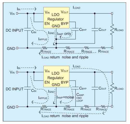
Figure 1: LDO wiring circuit solution
If an LDO input power source that drives the image processor is 3.6V from a single-cell lithium battery and 1.8V at a current of 200mA, the conversion efficiency is only 50%, so some hot spots are generated in the phone. Reduced battery operating time. Although these disadvantages do exist with respect to large input and output voltage differences, the situation is different when the voltage difference is small. For example, if the voltage drops from 1.5V to 1.2V, the efficiency becomes 80%.
When using a 1.5V mains supply and requiring a buck to 1.2V to power the DSP core, the switching regulator has no obvious advantage. In fact, switching regulators cannot be used to reduce 1.5V to 1.2V because the MOSFET cannot be fully boosted (either on-chip or off-chip). LDO regulators are also unable to accomplish this task because the dropout voltage is typically higher than 300mV.
The ideal solution is to use a VLDO regulator with an input voltage range close to 1V, a dropout of less than 300mV, and an internal reference close to 0.5V. Such a VLDO regulator can easily reduce the voltage from 1.5V to 1.2V with a conversion efficiency of 80%. Since the power level at this voltage is typically around 100 mA, a power loss of 30 mW is acceptable. The output ripple of the VLDO can be less than 1mVP-P. Low ripple is easily ensured by using VLDO as a post regulator for a step-down switching regulator.
Switching DC/DC Buck-Boost Regulator
The switching DC/DC buck-boost regulator is divided into a Buck switching DC/DC buck regulator, a Boost switching DC/DC boost regulator, and a voltage reduction from 4.2V to 2.5 according to the lithium battery. V can automatically switch the Buck-Boost switching DC/DC buck-boost regulator with step-down function. When the voltage difference between the input and output is high, the switching regulator avoids the efficiency issues of all linear regulators. It achieves efficiencies as high as 96% by using low-resistance switches and magnetic memory cells, thus greatly reducing power loss during conversion.
The Buck Switching DC/DC Buck Regulator is a constant frequency, current mode buck architecture with built-in main (P-channel MOSFET) and synchronous (N-channel MOSFET) switches. The PWM controlled oscillator frequency determines its operating efficiency and cost of use. Selecting a high switching frequency DC/DC can greatly reduce the size and capacity of external inductors and capacitors, such as high switching frequencies exceeding 2MHz. Switching regulators have fewer disadvantages and can often be overcome with good design techniques. However, the frequency leakage interference of the inductor is difficult to avoid, and the EMI radiation needs to be considered when designing the application.
Figure 2 shows the Buck switching DC/DC application circuit design, which requires the thick line part of the picture: the thick line is the channel of high current; select the high quality, low ESR X7R & X5R ceramics of MuRata, Tayo-Yuden, TDK&AVX Capacitors; in applications with high ambient temperatures, or low supply voltages and high duty cycle conditions (such as buck), consider the device's cooling and heat dissipation. It must be noted that SW vs. L1 distance <4mm; Cout vs. L1 distance <4mm; SW, Vin, Vout, GND lines must be short and short.
To get a stable and low-noise high-frequency switching regulator, you need to carefully arrange the layout of the PCB. All devices must be close to DC/DC. You can divide the PCB into several pieces according to function, as shown in Figure 3. 1. Keep the path between Vin and Vout, Cin and Cout are shorted to reduce noise and interference; 2. The feedback components of R1, R2 and CF must be kept close to the VFB feedback pin to prevent noise; 3. Large area Directly connect the 2 feet and the negative ends of Cin and Cout.
Figure 2: Buck Switching DC/DC Application Line Design
DC/DC application examples: 1. APS1006 powers MCU/DSP core (Core); 2. APS1006 is applied to electronic miner's lamp (Fig. 3); 3. APS1046 is applied to 0.8-1.8" micro hard disk power supply (Fig. 4); The APS1006 and APS4070 are used in smartphones (Figure 5).
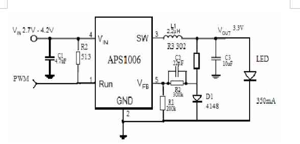
Figure 3: APS1006 applied to electronic miner's lamp
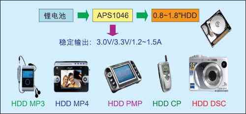
Figure 4: APS1046 is applied to 0.8-1.8" micro hard disk power supply
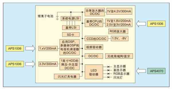
Figure 5: Application of APS1006 and APS4070 on smartphones
Charge pump and its application skills
The capacitive charge pump implements voltage boosting through a switch array and oscillator, logic, and comparison controllers, and uses capacitors to store energy. The charge pump is inductorless, but requires an external capacitor. Working at higher frequencies, small ceramic capacitors (1μF) can be used to minimize space usage and low cost of ownership. The charge pump provides ±2 times the output voltage with only an external capacitor. The loss is mainly due to the equivalent series resistance (ESR) of the capacitor and the RDS(ON) of the internal switching transistor.
The charge pump converter does not use an inductor, so its radiated EMI is negligible. The input noise can be filtered out with a small capacitor. Its output voltage is precisely pre-set during factory production, and the adjustment capability is realized by the on-chip on-chip linear regulator. Therefore, the charge pump can be designed to increase the number of switching stages of the charge pump as needed to provide enough for the back-end regulator. Activity space. The charge pump is ideal for the design of portable applications. From the internal structure of the capacitive charge pump, it is actually a system on chip.
A charge pump is a non-radiative, effective boost device that uses a capacitor as an energy storage device without the use of an inductor. When designing the application, you need to pay attention to the influence of the capacity and material of the capacitor on the output ripple. The capacity of the external capacitor is related to the output ripple. At a fixed operating frequency, too small a capacitor capacity will increase the output ripple. The output ripple size is related to the capacitor material medium, and the material type of the external capacitor is related to the output ripple. The same charge pump uses the same capacity and size as the result of the output ripple for different material types of capacitors. In the case where the operating frequency is fixed and the capacitor capacity is the same, an excellent material medium will effectively reduce the ripple. A low ESR X7R & X5R ceramic capacitor is a good choice.
LCD Module (LCM) is currently a large demand for CP, MP3/MP4, and PMP. In a limited PCB area, it needs to be equipped with LCD screen, digital camera lens and flash, audio DAC and other devices, so it needs to be packaged. A small multi-chip combination power module (MCM) to reduce the area of ​​the PCB occupied by the power IC, and mobile products require these power ICs to have almost no interference with RF.
Battery Charge Management Chip and Lithium Battery Protection IC
The Lithium Battery Charging IC is a system-on-chip (SoC) that consists of a read enable microcontroller, a 2x trickle charge controller, a current loop error amplifier, a voltage loop error amplifier, a voltage comparator, a temperature sensing comparator, Loop selection and multiplex driver, charge status logic controller, state generator, multiplexer, LED signal generator, MOSFET, reference voltage, power-on reset, undervoltage lockout, overcurrent/short circuit protection, etc. The functional IC is integrated on a wafer. It is a highly integrated, intelligent chip. Lithium-ion intelligent charging process: 涓æµå……--> constant current charging--> constant voltage charging--> voltage detection, so the key to circuit design is to do: full protection, full charging, automatic monitoring, automatic control.
The lithium battery protection circuit is packaged in a lithium battery pack, which consists of a lithium battery protection IC and two MOSFETs. In FIG. 6, OD stands for overdischarge control; OC stands for overcharge control; P+, P-connects charger; B+, B- connects lithium battery. The simple working principle of the lithium battery protection circuit is as follows: the normal state M1 and M2 are both turned on; when the overcharge is over, the M2 OC pin is turned from the high potential to the low potential, the electric gate is turned off, the charging is turned off, and the overcharge protection is realized; the charging current direction P+-- >P-; Over-discharge M1 OD pin turns from high potential to low potential, the electric gate is closed, the charge and discharge are cut off, and over-discharge protection is realized; the discharge current direction is P- --> P+.
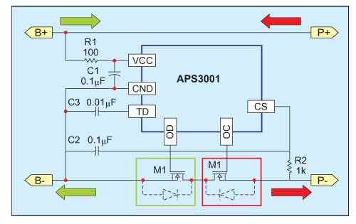
Figure 6: Lithium battery protection circuit
The PCB of the lithium battery protection circuit is very small. The design must pay attention to: 1. The MOSFET is as close as possible to B-, P-; 2. The ESD protection capacitor is as close as possible to P+, P-; 3. adjacent line spacing > 0.25 Mm, the line through which the current is large is to be widened, and the ground line is widened.
100% authentic best 18650 cells, below is our regular inventory list:
authentic sony li ion battery cells
US18650VTC6 3000mAh 15A/20AdischargeUS18650VTC5A 2500mAh 30Adischarge
US18650VTC5 2500mAh 20Adischarge
US18650VTC4 2100mAh 30Adischarge
US18650V3 2200mAh 10Adischarge E bike cells
US18650VC7 3400mAh 5A/8Adischarge
US18650NC1 2900mAh 10Adischarge E bike cells
US454261A8T 1590mAhlipo cells
Original Sanyo cells:
NCR18650BF 3400mAh
NCR18650GA 3450mAh 10AdischargeE bike cells
UR16650ZTA 2500mAh
UR18650ZTA 4.35V 3000mAh
UR18650FJ 2100/2200mAh red top
UR18650FM 2500/2600mAh blue head
UR18650FK 2300/2400mAh green top
UR18650ZY 2450/2550mAh Made In Japan
UR18650ZY 2450/2550mAh
UR18650AY 2150/2250mAh white head
UR14500P 830mah
UR18500F(K) 1620/1700mAh
UR18650NSX 2600mAh 20Adischarge
UF103450PN 1880/2000mAh with fuse
UF103450PN 1880/2000mAh no fuse
UF463450F
UF703450 1430/1480mAh
UF653450 1250/1300mAh
UF624447F 1530mAh
UF553450ZP 1150/1200mAh
UF553450ZP 1150/1200mAh
UF553443ZU 1000mAh
UF463048F
UF553436G
Authentic Panasonic cells:
NCR18650B3 3400mAh
NCR18650A 3100mAh
NCR18650BM 3200mAh
NCR18650 2900mAh
NCR18650PF 2900mAh 10AdischargeE bike cells
NCA103450 2350mAh no breaker
NCA903864 3120mAh
NC-1900SCR
NCR18500A 1940/2040mAh
NCR18650GA 3450mAh 10AdischargeE bike cells
Original Samsung li ion cells:
INR18650-25RM 2500mAh 20Adischarge
INR18650-25RM 2500mAh 20Adischarge
INR18650-25R 2500mAh 20Adischarge,
INR18650-20RM 2000mAh 22Adischarge
INR18650-30Q 3000mAh 15Adischarge
ICR18650-30B 4.35V 3000mAh
INR18650-35E 3500mAh 10Adischarge
INR18650-29E 2900mAh 8.25Adischarge
INR18650-32E 3200mAh 10Adischarge
ICR18650-22P 2150mAh 10Adischarge
ICR18650-22PM 2150mAh 10Adischarge,
ICR18650-22F 2200mAh
ICR18650-22FM 2200mAh
ICR18650-26JM 2600mAh
ICR18650-26FM 2600mAh
ICR18650-26HM 2600mAh
Original LG cells:
INR18650HE4, 2500mAh 20Adischarge
INR18650F1L, 3400mAh
ICR18650S3, 2200mAh,
ICR18650B4/B4L, 2600mAh
ICR18650MF1/MF2,2200mAh,10Adischarge
ICR18650M26,2600mAh, 10Adischarge
INR18650MG1 2900mAh 10Adischarge
INR18650MH1 3200mAh 10Adischarge
INR18650MJ1 3500mAh 10Adischarger
18650 Battery,Best 18650 Battery,18650 Lithium Battery,18650 Lithium Ion Battery
Asarke Industry Co., Limited , https://www.asarke-industry.com