Optimized design of 3GHz CMOS low noise amplifier
Abstract: Based on the 0.18 μm CMOS process, using a cascode source negative feedback structure, a 3 GHz low noise amplifier circuit is designed. The performance of the circuit is analyzed from the perspective of impedance matching and noise optimization, and the corresponding optimization design method is proposed. Simulation results show that the amplifier has good performance indicators, with a power gain of 23.4 dB, a reverse transmission coefficient of -25.9 dB, a noise figure of 1.1 dB, and a 1dB compression point of ﹣13.05 dBm.
1 Introduction
Modern wireless communication technology continues to develop in the direction of low cost and portable, making radio frequency integrated circuits based on CMOS technology become a research hotspot in recent years. In the design of radio frequency receivers, the optimal design of the front-end circuit is particularly critical in order to obtain good overall system performance. The low-noise amplifier (LNA) as the first functional module of the radio frequency receiver of the wireless communication system, its noise characteristics directly affect the sensitivity and signal-to-noise ratio of the entire receiver. It must provide sufficient power under certain power consumption conditions. Gain, excellent noise performance, good linearity and input and output matching. In the GHz frequency range, the CMOS process has the advantages of low price, high integration, and low power consumption compared with other processes. The use of the CMOS process to design RF integrated circuits has been more and more widely used. This article uses the CMOS process to achieve Optimized design for a 3 GHz low noise amplifier.
In the design of the LNA, several key parameters such as gain, noise figure, input impedance, and linearity should be dealt with by a compromise principle [1]. TH Lee proposed the design specifications under power constraints [2], and then many people have studied the design method of CMOS LNA [3-5]. This article mainly from the perspective of analysis of LNA input and output impedance matching and noise coefficient, for each influencing factor of the parameters, respectively, put forward optimization methods, and then comprehensively consider other indicators, designed a good performance of low noise amplifier , And conducted circuit simulation and layout design.
2 LNA structure
In the design of LNA, the cascode source negative feedback (Cascode) structure is widely used at present, as shown in Figure 1. In this structure, source negative feedback can not only achieve input impedance matching, but also improve the stability of the system, and has the characteristics of improving the linearity of LNA, and the cascade structure composed of M1 and M2 both improves the output impedance of the circuit , So that the gain of the circuit is greatly improved, and the reverse isolation of the circuit can be achieved [6], so that the output end and the input end do not affect each other, thereby facilitating the design of the LNA.
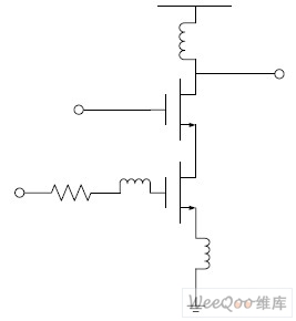
Figure 1 Negative feedback structure of cascode source
By adding a bias circuit on the basis of the above structure and optimizing and adjusting the circuit structure, a complete circuit structure can be obtained. The circuit structure realized in this paper is shown in Figure 2.

Figure 2 LNA circuit diagram
Transistors M1 and M2 form a Cascode structure. Since this structure does not consider the matching between the common source and the common gate, adding the inductance Lm between M1 and M2 can improve the matching between the two stages [7], which not only The power gain is improved, and the noise figure can also be improved [8]. At the same time, a capacitor C2 is connected in parallel between the gate and source of M1, which is used to adjust the capacitance Cgs between the gate and source, which is convenient to match the input impedance with Lg and Ls.
Transistors M3, M4 and M1, M2 together form a cascode current mirror [9], as a bias circuit, and the width of M3 and M4 should take a relatively small value to reduce the current consumed by the bias circuit. Resistor R2 should be large enough to reduce the noise current caused by the bias circuit. Resistor R1 is used to adjust the gate-source voltage and drain current of input transistor M1 to determine the static power consumption. Capacitor C1 can make the gate of M2 AC connected. voltage. Cin and Cout are DC blocking capacitors.
3 LNA performance optimization
3.1 Input and output matching
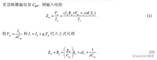
The small-signal equivalent circuit of the LNA input with source negative feedback is shown in Figure 3, where gm is the transconductance of M1 and Cgs is obtained by paralleling the gate-source capacitances Cgs1 and C2 of M1.
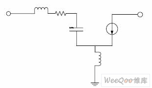
Figure 3 Small-signal equivalent circuit of source negative feedback structure

4 Circuit simulation and layout design
The simulation uses TSMC's 0.18 μm CMOS process, the simulation environment is Cadence SpectreRF, and the power supply voltage is 2V. The simulation results are shown in Figure 5.

It can be seen from Figure 5 (a) that the power gain of the designed low-noise amplifier reaches 23.4 dB at 3 GHz, which satisfies the power gain requirement well. In Figure 5 (b), the input reflection coefficient S11 reaches -25.9 dB, showing good input impedance matching. Figure 5 (c) shows that after the noise optimization, the noise figure of the circuit is only 1.1 dB, and the 1dB compression point in Figure 5 (d) is -13.05 dBm, indicating that the low noise amplifier has good linearity.
Using the 0.18 μm CMOS process model, cadence virtuoso software is used to design the layout of the LNA. As shown in Figure 6, the layout size is 0.485 mm × 0.395 mm.
5 Conclusion
In this paper, through the analysis of the cascode structure, the performance of the circuit is optimized from the perspective of impedance matching, noise figure and linearity, and a 3 GHz low noise amplifier is designed. Under 0.18 μm CMOS process, the circuit was simulated using Cadence SpectreRF software. The results show that the LNA's power gain, impedance matching, noise figure, and linearity have achieved good performance. Finally, the layout design of LNA was carried out.
The author's innovation in this paper: Based on the analysis of the cascode structure, the circuit structure of the LNA is improved, and the method of adding inductance between the cascode structure to improve the noise figure and the parallel capacitance to increase the input impedance matching is proposed. The design of low noise amplifier has certain reference value.
Kitchen Appliance,Small Kitchen Appliance Cooker,Counter Top Electric Cooker,Electric Hotplate Cooker
Shaoxing Haoda Electrical Appliance Co.,Ltd , https://www.zjhaoda.com