Abstract: DC-DC converters are an excellent source of electric fields and magneTIc fields. Their EMI spectrum begins at the switching frequency and often extends over 100MHz. To minimize capaciTIve couplings and magneTIc couplings care must be exercised in printed circuit board (PCB) layout . ParasiTIc capacitance and parasitic inductance of the circuit must be evaluated so that the proper trade-off can be made early in the design phase.
For many years, repeated introductions of integrated DC-DC power-supply controllers have given us ever-higher levels of performance. These ICs unburden the systems engineer by removing the task of power-supply design, but this simplification has led to a loss of knowledge. Switching converters should therefore serve as a reminder to be careful. The following discussion presents rules for avoiding surprises when designing board layouts for non-isolated DC-DC converters.
The first rule in optimizing such a layout is to isolate the converter. DC-DC converters are an excellent source of electric and magnetic fields. Their EMI spectrum begins at the switching frequency and often extends over 100MHz. To minimize capacitive couplings and "magnetic- field-to-loop "couplings, you should locate the converter away from other circuitry, especially from low-level analog circuitry.
Isolating the converter is not always easy. Some boards accept input voltage on one side of the converter and distribute output voltages on the other side. VME cards or telecom cards, for example, include very complex routings with currents as high as 20A. A single connector brings in the input voltage and distributes several output voltages to the backplane. Therefore, there's a strong temptation to place the converter near this connector to reduce resistive drop. The area, however, is dense with interface drivers, backplane buses, and so forth , with the associated risk of noise coupling. A power connector can be added in some cases, but that solution entails extra board area and cost.
Resistance in the copper traces is the most constraining factor. For a trace of a given length and thickness, this resistance is R = Ï Ã— (l / S) where l is the trace length in meters, S is the trace area in square meters , and Ï (the resistivity of copper) is 1.7x10⁻⁸Ω-m at 20 ° C, or 2.1 x 10⁻⁸Ω-m at 70 ° C. As an example, the resistance of a copper trace 0.5cm wide and 35µm thick at 20 ° C is 1mΩ / cm. That value may appear negligible, but it commands attention if you are distributing 2.5V at 10A through two connectors and a backplane board.
On some boards, the trace thickness includes a tin-lead layer. This layer can nearly double the equivalent resistance: lead resistivity = 2.07 x 10⁻⁷Ω-m at 20 ° C
tin resistivity = 1.14 x 10⁻⁷Ω-m at 20 ° CA trade-off between accuracy and trace loss lets you move the converter away from the connector. You can limit the effect of a resistive drop by performing a remote VOUT measurement near the connector , but beware of capactive couplings! To confine large currents to a defined area, route all the supply lines through pins at one end of the connector.
MOSFET DriversAs switching frequencies increase, the switching time becomes shorter and shorter: typically 10ns for a 500kHz converter. At that frequency, even the shortest trace has a significant impedance. It's also important to note that a peak gate current can rise to several amperes in an extremely short time. Therefore, the proper routing of MOSFET-drive signals begins with an analysis of the converter's block diagram.
For example, consider a synchronous step-down controller for notebook computers (Figure 1). The MOSFETs are driven by the transference of energy from the tank capacitors (C6 and C7) to the gates through the few ohms of the driver outputs. Note that the gate drive for the high-side n-channel MOSFET (Q1) is floating. The n-channel driver works like a charge pump!
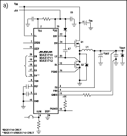
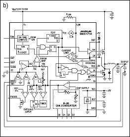
More Detailed Image.
Figure 1. Operation of the MAX1710 synchronous step-down controller is depicted by an application circuit (a) and an internal block diagram (b).
Figure 2 highlights the current paths during turn-on. Any series inductance can lead to disaster. In the best case, the spikes are higher, but simply increase the switching losses. In the worst case, the two MOSFETs can blow up due to cross conduction (simultaneous turn-on). Consequently, an optimal routing implies very short and wide traces between: C6 and Vdd
C6 and Q2 (S)
C7 and BST, and C7 and LX
Q1 (G) and DH
Q2 (G) and DL
Q1 (S) and LX
Q2 (S) and PGND Keep in mind that the parasitic inductance for a 1cm trace is about 10nH.
Looking closely at C6, you can see that it supplies Q1 and Q2, but not in the same way. It acts as a filter capacitor for Q1 and as a tank capacitor for Q2. Because we cannot place C6 near the high-side and low -side drivers at the same time, we place it as close as possible to Vdd and PGND (where the peak currents flow), and also near C7 (almost average current). Notice that the PGND, DL, and Vdd pins are side by side, and not by chance! Q2 and C6 are placed to minimize the ground-trace lengths between PGND, C6 (-), and Q2 (S). Connect this ground trace to the ground plane at a single point, near the PGND pin . To avoid common-impedance coupling, LX should be connected to Q1, and PGND / C6 (-) to the source of Q2. Figure 3 highlights the current paths during turn-off.
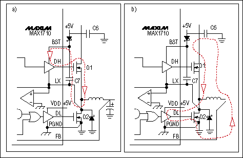
Figure 2. The dotted lines indicate heavy current flow in the gate-drive circuits for Q1 (a) and Q2 (b).
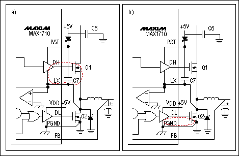
Figure 3. The dotted lines indicate heavy current flow in the gate-discharge (turn-off) paths for Q1 (a) and Q2 (b).
The number of "via" should be limited as much as possible. Indeed, the few tens of nanohenries added by a via is embarrassing when di / dt is high. For that reason, you should place all power components on the component layer, even the SMD ones. If you have no other choice, put several via in parallel.
We must remember that controllers are often oversized for the application at hand. Common practice, for instance, employs a 10A controller to produce a 3A output. Because we generally choose minimum-sized MOSFETs for cost reasons, the on-chip drivers remain oversized and Therefore capable of more gate drive than is necessary.
Because the earlier discussion sought to avoid slowing the MOS gate drive, it seems paradoxical to place a small (10Ω to 100Ω) resistor in series with the gate drive. Oversized and / or fast drive waveforms, however, produce more switching noise and RF interference . At the other extreme, slow waveforms produce more switching loss in the MOSFET (s) and diode (if any). A good compromise is to reduce EMI by slowing the waveform slopes as much as possible, while maintaining an acceptable level of efficiency. (Components in the gate drive of Figure 4b let you trim the rise and fall times separately.) Fortunately, large drivers allow a final bit of optimization.
Routing the Power StageFigure 4 illustrates the two high-current loops common to many power converters. In responding to the perturbations caused by switching, these loops support high di / dt, and (at some nodes) high dv / dt as well. Identifying these loops helps to reduce their effects. Note that di / dt is great within the converter (at the switching node) but small outside the converter. Indeed, currents before the input capacitor and after the output capacitor reach a high value, but they are nearly continuous. Their AC components are low when the converter is well designed.
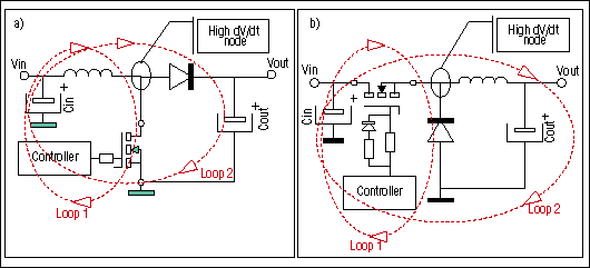
Figure 4. These simple schematics illustrate the basic operation of the step-up (a) and step-down (b) switching converters.
First, minimize parasitic inductance. We will consider a step-up converter, but the reasoning can be transposed for a step-down type. Figure 5 illustrates the kinds of parasitic inductance that cause the most problems.
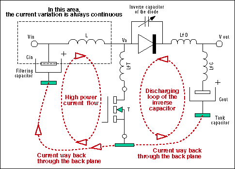
Figure 5. When the main switching transistor (T) turns off, the diode capacitance discharges as shown.
Without describing the 10 phases of a switching cycle, we can consider the MOSFET turn-off, when inductor current has been short-circuited by the MOSFET. The diode's inverse capacitor charges extremely fast via loop two, and the node-voltage Va at the diode's anode (normally at Vout-Vd) goes to near 0V. The serial inductors (LfT + LfD + LfC) increase this discharge time, thereby increasing switching loss in the MOSFET. These types of inductance also generate noise.
Peak current is limited by the transistor, which operates as a current source (Vds still equals a few volts). For a 2A MOSFET, this current source could be 10A! The current level is large for a very short time (a few 10ns) . Remember that varying the current through an inductor produces a voltage proportional to the current variation: v = L × [di (t) / dt] This transition phase is a good spike generator! Once more, we minimize parasitic inductance by minimizing trace lengths and using short, wide traces around the MOSFET, diode, and Cout. You can now see how noise can be reduced by the control of slopes in the gate-drive waveforms.
To limit resistive voltage drops and the number of via, power-stage SMD components should be placed on the component side of the board and power traces routed on its component layer. If possible, the power ground should also be routed on the same layer. This arrangement has another benefit: less perturbation of the ground plane. To cancel radiated fields, take care to minimize the area of ​​the power-current loop.
When it becomes necessary to route a power trace on a layer other than the component layer, choose a trace from the inductor or filter capacitors (ie, Cout for a step-down converter, or Cin for a step-up converter). Because current through such traces is nearly continuous, it produces no noise, just a resistive drop. Parasitic inductance will be smaller if you route this trace on the layer just under the component layer. To avoid coupling by common impedance, you should separate PGND, the power -circuit ground, and the general ground plane (Figure 6).
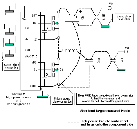
Figure 6. These details illustrate the routing of PGND versus gate-control traces in the controller circuit.
Capacitors and Other ComponentsIt's important to pay close attention to the routing of traces from capacitor terminals in a DC-DC converter circuit. Large-valued low-ESR capacitors are expensive, and bad routings can cancel their performance. A good routing, on the other hand, can lower the output noise from 150mV to 50mV!
Ripple is directly related to the inductor value, the capacitor ESR, the switching frequency, and so forth, but HF noise (spikes) depend on parasitic elements and the switching action. We can anticipate spikingfrequencies from 1MHz to 10MHz, depending on the switching frequency .
In a bad routing (Figure 7a), parasitic inductance associated with trace lengths causes trouble: L1 brings about an increase in noise, and L2 limits the attenuation of HF capacitor CoHF. The fix (Figure 7b) is to bring the input trace in on one side of the capacitor pad, and the output trace out on the other side of the pad.
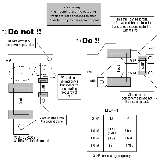
Figure 7. Improper routing of capacitor traces introduces unwanted parasitic inductance.
Now, having placed and routed the bulkiest parts, we turn our attention to the inductor. A deliberate but unwanted coupling (Figure 8a) allows current in the power loop to pollute the controller supply (Vcc). High di / dt produced by switching through Lp1 causes Vcc overshoots that easily reach several hundred millivolts. Using
v (t) = L × [di (t) / dt] with L = 10nH, ΔI = 1A, and Δt = 50ns, ΔV = 0.2V!
As mentioned earlier, the first precaution is to separate the power traces and be careful with PGND. The second precaution is to avoid connecting traces to the power loop (see Figure 8b). Traces that distribute the input voltage should be connected before the input capacitor and the controller's Vcc connection. Output voltage is distributed after the connections to the HF output capacitor.
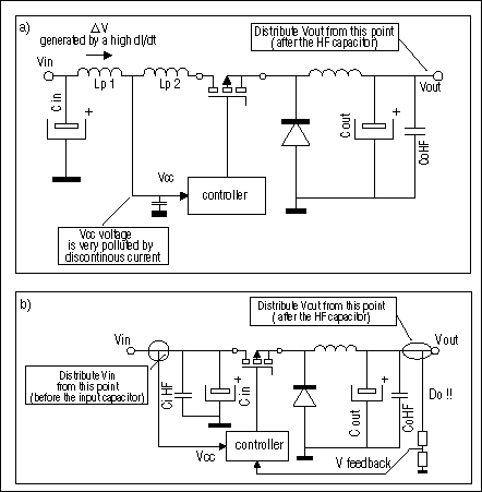
Figure 8. Unwanted common-impedance coupling (a) is prevented by the connections shown in (b).
Finally, some miscellaneous advice: Bad routing of the PGND trace can cause common-impedance coupling (one reason for the PGND terminal is to avoid polluting the controller's internal ground node). Move high-impedance traces (especially the output resistor divider that adjusts the output voltage) away from nodes that support high dV / dt. Currents induced by such coupling can make the controller oscillate.
For many years, repeated introductions of integrated DC-DC power-supply controllers have given us ever-higher levels of performance. These ICs unburden the systems engineer by removing the task of power-supply design, but this simplification has led to a loss of knowledge. Switching converters should therefore serve as a reminder to be careful. The following discussion presents rules for avoiding surprises when designing board layouts for non-isolated DC-DC converters.
The first rule in optimizing such a layout is to isolate the converter. DC-DC converters are an excellent source of electric and magnetic fields. Their EMI spectrum begins at the switching frequency and often extends over 100MHz. To minimize capacitive couplings and "magnetic- field-to-loop "couplings, you should locate the converter away from other circuitry, especially from low-level analog circuitry.
Isolating the converter is not always easy. Some boards accept input voltage on one side of the converter and distribute output voltages on the other side. VME cards or telecom cards, for example, include very complex routings with currents as high as 20A. A single connector brings in the input voltage and distributes several output voltages to the backplane. Therefore, there's a strong temptation to place the converter near this connector to reduce resistive drop. The area, however, is dense with interface drivers, backplane buses, and so forth , with the associated risk of noise coupling. A power connector can be added in some cases, but that solution entails extra board area and cost.
Resistance in the copper traces is the most constraining factor. For a trace of a given length and thickness, this resistance is R = Ï Ã— (l / S) where l is the trace length in meters, S is the trace area in square meters , and Ï (the resistivity of copper) is 1.7x10⁻⁸Ω-m at 20 ° C, or 2.1 x 10⁻⁸Ω-m at 70 ° C. As an example, the resistance of a copper trace 0.5cm wide and 35µm thick at 20 ° C is 1mΩ / cm. That value may appear negligible, but it commands attention if you are distributing 2.5V at 10A through two connectors and a backplane board.
On some boards, the trace thickness includes a tin-lead layer. This layer can nearly double the equivalent resistance: lead resistivity = 2.07 x 10⁻⁷Ω-m at 20 ° C
tin resistivity = 1.14 x 10⁻⁷Ω-m at 20 ° CA trade-off between accuracy and trace loss lets you move the converter away from the connector. You can limit the effect of a resistive drop by performing a remote VOUT measurement near the connector , but beware of capactive couplings! To confine large currents to a defined area, route all the supply lines through pins at one end of the connector.
MOSFET DriversAs switching frequencies increase, the switching time becomes shorter and shorter: typically 10ns for a 500kHz converter. At that frequency, even the shortest trace has a significant impedance. It's also important to note that a peak gate current can rise to several amperes in an extremely short time. Therefore, the proper routing of MOSFET-drive signals begins with an analysis of the converter's block diagram.
For example, consider a synchronous step-down controller for notebook computers (Figure 1). The MOSFETs are driven by the transference of energy from the tank capacitors (C6 and C7) to the gates through the few ohms of the driver outputs. Note that the gate drive for the high-side n-channel MOSFET (Q1) is floating. The n-channel driver works like a charge pump!
More Detailed Image.
Figure 1. Operation of the MAX1710 synchronous step-down controller is depicted by an application circuit (a) and an internal block diagram (b).
Figure 2 highlights the current paths during turn-on. Any series inductance can lead to disaster. In the best case, the spikes are higher, but simply increase the switching losses. In the worst case, the two MOSFETs can blow up due to cross conduction (simultaneous turn-on). Consequently, an optimal routing implies very short and wide traces between: C6 and Vdd
C6 and Q2 (S)
C7 and BST, and C7 and LX
Q1 (G) and DH
Q2 (G) and DL
Q1 (S) and LX
Q2 (S) and PGND Keep in mind that the parasitic inductance for a 1cm trace is about 10nH.
Looking closely at C6, you can see that it supplies Q1 and Q2, but not in the same way. It acts as a filter capacitor for Q1 and as a tank capacitor for Q2. Because we cannot place C6 near the high-side and low -side drivers at the same time, we place it as close as possible to Vdd and PGND (where the peak currents flow), and also near C7 (almost average current). Notice that the PGND, DL, and Vdd pins are side by side, and not by chance! Q2 and C6 are placed to minimize the ground-trace lengths between PGND, C6 (-), and Q2 (S). Connect this ground trace to the ground plane at a single point, near the PGND pin . To avoid common-impedance coupling, LX should be connected to Q1, and PGND / C6 (-) to the source of Q2. Figure 3 highlights the current paths during turn-off.
Figure 2. The dotted lines indicate heavy current flow in the gate-drive circuits for Q1 (a) and Q2 (b).
Figure 3. The dotted lines indicate heavy current flow in the gate-discharge (turn-off) paths for Q1 (a) and Q2 (b).
The number of "via" should be limited as much as possible. Indeed, the few tens of nanohenries added by a via is embarrassing when di / dt is high. For that reason, you should place all power components on the component layer, even the SMD ones. If you have no other choice, put several via in parallel.
We must remember that controllers are often oversized for the application at hand. Common practice, for instance, employs a 10A controller to produce a 3A output. Because we generally choose minimum-sized MOSFETs for cost reasons, the on-chip drivers remain oversized and Therefore capable of more gate drive than is necessary.
Because the earlier discussion sought to avoid slowing the MOS gate drive, it seems paradoxical to place a small (10Ω to 100Ω) resistor in series with the gate drive. Oversized and / or fast drive waveforms, however, produce more switching noise and RF interference . At the other extreme, slow waveforms produce more switching loss in the MOSFET (s) and diode (if any). A good compromise is to reduce EMI by slowing the waveform slopes as much as possible, while maintaining an acceptable level of efficiency. (Components in the gate drive of Figure 4b let you trim the rise and fall times separately.) Fortunately, large drivers allow a final bit of optimization.
Routing the Power StageFigure 4 illustrates the two high-current loops common to many power converters. In responding to the perturbations caused by switching, these loops support high di / dt, and (at some nodes) high dv / dt as well. Identifying these loops helps to reduce their effects. Note that di / dt is great within the converter (at the switching node) but small outside the converter. Indeed, currents before the input capacitor and after the output capacitor reach a high value, but they are nearly continuous. Their AC components are low when the converter is well designed.
Figure 4. These simple schematics illustrate the basic operation of the step-up (a) and step-down (b) switching converters.
First, minimize parasitic inductance. We will consider a step-up converter, but the reasoning can be transposed for a step-down type. Figure 5 illustrates the kinds of parasitic inductance that cause the most problems.
Figure 5. When the main switching transistor (T) turns off, the diode capacitance discharges as shown.
Without describing the 10 phases of a switching cycle, we can consider the MOSFET turn-off, when inductor current has been short-circuited by the MOSFET. The diode's inverse capacitor charges extremely fast via loop two, and the node-voltage Va at the diode's anode (normally at Vout-Vd) goes to near 0V. The serial inductors (LfT + LfD + LfC) increase this discharge time, thereby increasing switching loss in the MOSFET. These types of inductance also generate noise.
Peak current is limited by the transistor, which operates as a current source (Vds still equals a few volts). For a 2A MOSFET, this current source could be 10A! The current level is large for a very short time (a few 10ns) . Remember that varying the current through an inductor produces a voltage proportional to the current variation: v = L × [di (t) / dt] This transition phase is a good spike generator! Once more, we minimize parasitic inductance by minimizing trace lengths and using short, wide traces around the MOSFET, diode, and Cout. You can now see how noise can be reduced by the control of slopes in the gate-drive waveforms.
To limit resistive voltage drops and the number of via, power-stage SMD components should be placed on the component side of the board and power traces routed on its component layer. If possible, the power ground should also be routed on the same layer. This arrangement has another benefit: less perturbation of the ground plane. To cancel radiated fields, take care to minimize the area of ​​the power-current loop.
When it becomes necessary to route a power trace on a layer other than the component layer, choose a trace from the inductor or filter capacitors (ie, Cout for a step-down converter, or Cin for a step-up converter). Because current through such traces is nearly continuous, it produces no noise, just a resistive drop. Parasitic inductance will be smaller if you route this trace on the layer just under the component layer. To avoid coupling by common impedance, you should separate PGND, the power -circuit ground, and the general ground plane (Figure 6).
Figure 6. These details illustrate the routing of PGND versus gate-control traces in the controller circuit.
Capacitors and Other ComponentsIt's important to pay close attention to the routing of traces from capacitor terminals in a DC-DC converter circuit. Large-valued low-ESR capacitors are expensive, and bad routings can cancel their performance. A good routing, on the other hand, can lower the output noise from 150mV to 50mV!
Ripple is directly related to the inductor value, the capacitor ESR, the switching frequency, and so forth, but HF noise (spikes) depend on parasitic elements and the switching action. We can anticipate spikingfrequencies from 1MHz to 10MHz, depending on the switching frequency .
In a bad routing (Figure 7a), parasitic inductance associated with trace lengths causes trouble: L1 brings about an increase in noise, and L2 limits the attenuation of HF capacitor CoHF. The fix (Figure 7b) is to bring the input trace in on one side of the capacitor pad, and the output trace out on the other side of the pad.
Figure 7. Improper routing of capacitor traces introduces unwanted parasitic inductance.
Now, having placed and routed the bulkiest parts, we turn our attention to the inductor. A deliberate but unwanted coupling (Figure 8a) allows current in the power loop to pollute the controller supply (Vcc). High di / dt produced by switching through Lp1 causes Vcc overshoots that easily reach several hundred millivolts. Using
v (t) = L × [di (t) / dt] with L = 10nH, ΔI = 1A, and Δt = 50ns, ΔV = 0.2V!
As mentioned earlier, the first precaution is to separate the power traces and be careful with PGND. The second precaution is to avoid connecting traces to the power loop (see Figure 8b). Traces that distribute the input voltage should be connected before the input capacitor and the controller's Vcc connection. Output voltage is distributed after the connections to the HF output capacitor.
Figure 8. Unwanted common-impedance coupling (a) is prevented by the connections shown in (b).
Finally, some miscellaneous advice: Bad routing of the PGND trace can cause common-impedance coupling (one reason for the PGND terminal is to avoid polluting the controller's internal ground node). Move high-impedance traces (especially the output resistor divider that adjusts the output voltage) away from nodes that support high dV / dt. Currents induced by such coupling can make the controller oscillate.
custom logo:please send me your logo,and we will printed them on the credit Card USB Flash Drive which is a good idea of your company to do promotion gifts,This item is very popular.
The best gifts for company promotion/Wedding gift,you can not miss this card usb in such situation.
Selling Point:
1.We promise all USB Flash Drive is real full capacity.
2.The chip 100% test before production.
3.Free design for custom logo.
4.Free sample for small capacity ,just pay for the shipping cost.
USB Flash Drive Card,Card USB Flash Drive,USB Business Card,USB Pen Drive
Custom Usb Gift company limited , https://www.customusbgift.com