Design of multi-system radar signal source based on AD9959
With the development of radar technology, radars of various systems have emerged, such as pulsed Doppler radar, SAR, and phased array radar. Although these radars have different functions, in order to increase the range and the resolution of the upward range, all The large-scale wideband signal is colored.
In the field of radar signal source design, DDS technology and devices have been greatly developed. Correspondingly, many DDS devices with excellent performance have appeared. This article aims to introduce a new multi-system radar signal source based on AD9959 designed by Analog Devices. Design method, the device has the characteristics of high stability, flexible adjustment of phase, frequency and amplitude, and can generate 4 related signals at the same time. The signal form can be set arbitrarily. These excellent performances have been demonstrated in the development of radar signal sources. Good application prospects.
2 System hardware design
The multi-system radar signal source designed in this paper is based on ADI's AD9959, combined with FPGA control circuit and signal amplification circuit. The signal parameters are sent by the main control computer through the serial port and received with the FPGA to control the AD9959 to complete the corresponding signal output. In the actual launch process of the radar, most of them use pulse signals with large time and wide bandwidth. Therefore, in the architecture of the system hardware design, FPGA also completes a certain pulse output function to pulse the continuous wave signal output by the AD9959. Modulation, so as to achieve the ability to output radar pulse signals, and the output intermediate frequency signal can reach the frequency band required for radar transmission through the mixing circuit.
2.1 Introduction to AD9959 chip
AD9959 is a DDS chip with excellent performance, mainly reflected in the following aspects:
4 simultaneous output channels;
Each channel has independent frequency / phase / amplitude control function;
Super strong isolation between channels (> 65 dB);
Linear frequency / phase / amplitude scanning capability;
Capable of up to 16 levels of frequency / phase / amplitude modulation capability;
The power saving mode can be controlled by hardware / software.
The AD9959 provides multiple configuration functions through serial I / O. Based on a SPI mode provided by this serial I / O, it is compatible with previous ADI DDS devices. At the same time, the device uses advanced design technology, so that the device not only has excellent performance, but also has the characteristics of low power consumption. The device integrates 4 high-speed 10-bit DACs with outstanding broadband and narrow-band SFDR characteristics. Each channel has a 32-bit frequency control word, a 14-bit phase control word, and a 10-bit output amplitude control word. REF CLK can reach up to 500 M / s, and the PLL frequency multiplier can be set between 4 and 20 through software programming. Because the AD9959 has the ability to output multi-channel related signals, the AD9959 can be widely used in various occasions.
2.2 System configuration
The user transmits the parameters of the generated signal to the FPGA through the computer. After receiving the corresponding parameters, the FPGA controls the AD9959 to output the corresponding radar signal. Since the output signal of the AD9959 is a differential current signal, the 1: 1 transmission transformer is used in the system design The differential current signal is converted into a single-ended voltage signal. At the same time, in order to improve the output drive capability of the system, signal amplification is performed behind the transformer. The system block diagram is shown in Figure 1. 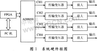
2.3 System communication interface and protocol
The system mainly sends commands to the AD9959 by the FPGA to output the corresponding signals. The control of the AD9959 is mainly realized through the serial bus SCLK and SDIO, where the maximum clock speed of SCLK can reach 200 MHz, and the AD9959 can pass the SDIO 4 The root data line (SDIO 0 ~ SDIO 3) simultaneously transmits data, so that the data throughput can be changed to 800 Mb / s. Previously, DDS products of Analog Devices had parallel and serial control modes, such as AD9850 and AD9959. The SPI control mode is undoubtedly more concise and more convenient for user control. AD9959 has 4 kinds of serial control transmission modes, namely Single-Bit Serial (2 and 3-wire) Modes, 2-Bit Serial Mode, 4-Bit SerialMode. The four output channels of the AD9959 share registers 0x03 to 0x18. This register address sharing mode enables four channels to write control words simultaneously. For example, to make all four channels of the AD9959 output a certain frequency, you only need to write to the AD9959 once through the serial bus. If the four channels are operated independently of each other, they can be selected through the channel selection register (CSR).
The serial working mode of AD9959 works in register level transmission, not byte level transmission. However, the SYNC I / O function provided by the AD9959 can interrupt the I / O operation. This mode allows a byte of the register to be set, thereby reducing the setting time. All commands are written on the rising edge of SCLK and read on the falling edge of SCLK. In the radar signal source designed in this paper, the single-bit serial 2-wire mode is adopted for the control mode of AD9959. In this working mode, AD9959 uses SDIO 0 as the data transmission pin. To make AD9959 work in this mode In this mode, you can set CSR <2: 1> in the CSR register to 00. In Single-Bit Serial 2-wire Mode transmission mode, it supports MSB first and LSB first.
The system operates the AD9959 through FPGA, which is mainly divided into two stages. The first stage is the instruction cycle. In this stage, the instruction is written into the AD9959, and a bit is written on each rising edge of SCLK. The section specifies whether the transfer to be performed is a read operation or a write operation, and also contains the register address; the second stage is the data transfer cycle, which mainly transfers the control words of the waveform parameters.
The sequential logic control completed in the figure is mainly implemented by FPGA. The specific signal parameters are sent to FPGA through the serial port through the host computer. Therefore, FPGA also completes the serial port transceiver function. Through the serial port, the system main controller (FPGA) can not only complete the control The host computer receives the command parameters, writes the signal parameters into the AD9959, and can also read out the internal state information of the AD9959 and upload it to the computer through the serial port.
3 System software design
3.1 FPGA programming
In the radar signal source designed in this article, the XINUNXSpartan-3 series FPGA is used, the model is XC23S1000, he has 106 logic gates, Distributed RAM total 120 kb, Block RAM total 432 kb, and also has 4 DCM units, the maximum available I / O391. Because the system uses FPGA as the core control device, it has good scalability. When the system parameters are changed, only the FPGA internal program needs to be modified. Instead of making hardware changes, it is precisely because FP-GA has such advantages that it makes this system very flexible.
Through programming to FPGA, the control function of AD9959 and the function of serial port transceiver are mainly completed. Four DDS cores are integrated inside the AD9959, and each DDS core integrates a 32-b phase accumulator and a phase-to-amplitude converter. The signal frequency of each DDS output can be calculated by the following formula: ![]()
Among them, fs represents the system sampling clock, FTW represents the frequency control word, and fo represents the frequency of the DDS output signal. Because in the radar signal source, the linear frequency modulation signal is a commonly used signal form, so here mainly take the linear frequency modulation signal as a reference. The FPGA can send a control word to the AD9959, which can control the starting frequency, frequency modulation slope coefficient, and cutoff frequency of the output signal. FPGA control AD9959 write instruction sequence logic diagram shown in Figure 2.
FPGA not only completes the function of controlling the AD9959 in the system, but also completes the function of transmitting serial port data in accordance with the RS232 protocol. The UART functions are described in Verilog HDL language, which makes the system more compact and compact.
3. 2 PC programming
The PC software mainly completes the input of user parameters and sends the data to the FPGA through the RS232 serial port. The program is written in C. Various parameters for generating radar signals can be entered on the interface, such as signal frequency, start frequency, cutoff frequency, frequency modulation slope, Since AD9959 can generate FSK, PSK, ASK multiple system signals, users can also select the signal style through the drop-down list. The system control software world is shown in Figure 3. 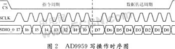
The serial communication control AcTIvex provided in Visual Studio.NET in the software realizes the serial data communication function. The program flow of the software is shown in Figure 4. 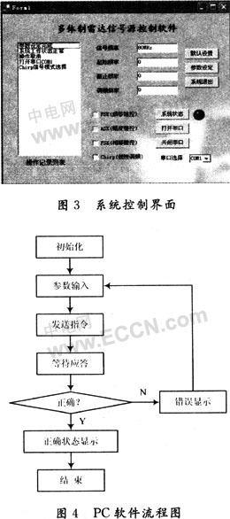
4 Conclusion
The system uses FPGA as the core controller, which not only completes the control function of AD9959, but also completes the serial data transmission function, which makes the circuit design more concise and has good scalability. During the system upgrade process, there is no need to change the hardware design , Only need to modify the FPGA internal program to complete the new function.
The radar signal source designed in this paper has been well applied in actual work. The system can output 4 coherent signals at the same time, with a frequency range of 10 to 150 MHz. Each output can be controlled individually or as a whole. The user can The signal parameters and patterns of the system output are determined through a PC, so that the corresponding radar signal can be easily output. The system has strong practicability, flexibility and expansibility, has achieved good results in practical work, and has good application prospects.
[Super bright with multiple modes]Powerful Cree LED Torch generates a brilliant large area floodlight or a perfect focused spotlight. Adjustable focus with 3 or 5 modes.
[High quality]This Aluminum Led Flashlight body is built of high quality aluminum, and it has a very solid construction,High-Efficiency and Great Output LED Chip.
[Easy to carry and charge]Easy to carry as a backup tool and small enough to put in your pocket, handbag, drawer, or car compartment. This Aluminum LED Flashlight takes standard AAA/AA or 18650 rechargeable battery.
[Waterproof and Shockproof]Anti-slip handle designing,make this flashlight perfect for using in the rain, snow or other emergency situations. It also can be used in wet condition or light rain day
Aluminum LED Flashlight
Portable Lights,Carbon Fiber Flashlight,Cree Led Flashlight,Multi Function Aluminum Torch
Ningbo Henglang Import & Export Co.,Ltd , https://www.odistarflashlight.com