Abstract: This applicaTIon note examines the effect of the output filter on audio Class D amplifier performance. Switch-mode amplifiers such as the MAX4295 and MAX4297 offer improved efficiency over their more tradiTIonal Class AB counterparts. By understanding the operaTIon of these devices, the modulaTIon noise spectrum and the loudspeaker loads they are required to drive, it is possible to completely eliminate the output filter while retaining the efficiency benefits of Class D amplifiers.
This article examines the output filter often required with a switch-mode (class D) audio power amplifier. Such filters not only maintain efficiency, they also suppress RF interference produced by fast output transitions. Each of the following circuits, based on Maxim's MAX4295 / MAX4297 amplifiers, can be optimized for a given application if the designer is aware of the tradeoffs involved. The amplifiers operate from a single supply in the range + 2.7V to + 5.5V, and they drive bridge-tied 4Ω loads with continuous power as high as 2W, with efficiency exceeding 85%. That performance makes them attractive as speaker drivers for portable equipment in which the battery life is limited.
The main advantage of class D amplifiers is their efficiency, which is higher than that of class AB amplifiers. As a minimum condition for achieving that efficiency, the load of a class D amplifier should present a high impedance at the switching frequency. In typical output waveforms (Figure 1) the duty cycle of the OUT + terminal varies but its pulse period is constant (the "ticks" shown between the two waveforms denote equal time periods). A running average of these pulses forms a slowly rising voltage (dashed line) over the sequence shown. Because the OUT- signal is the inverse of OUT +, it produces a slowly falling voltage. If the load is a speaker, in which the load is connected between the + and-terminals, this slow-moving component is audible but the high-frequency content is not reproduced.
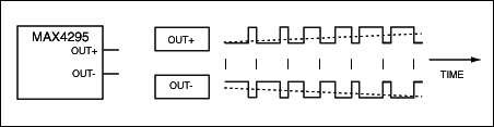
Figure 1. These complementary PWM outputs are generated by a class D amplifier in the bridge configuration (like the MAX4295). The average values ​​of these waveforms (the dashed lines) are produced by an output filter, whose loss and distortion-producing artifacts should be held to a minimum.
Whether to use an output filter or not depends on many factors. Consider the following: the MAX4295 / MAX4297 audio power amplifiers contain complementary output MOSFETs that implement pulse-width modulation (PWM). The duty cycles for the output waveforms from these devices are approximately 50% with zero input signal applied, and to maintain reasonable efficiency the MOSFETs should drive a high impedance at the switching frequency. Otherwise, when a resistor is connected directly across the outputs with no other components present, the output stages conduct almost 100% of the time regardless of changes in the duty cycle.
Now consider the impedance plot of a speaker such as an 8Ω, 1.75 "cone transducer, for which the MAX4295 / MAX4297 amplifiers are suitable drivers (Figure 2). The speaker impedance rises beyond the audio band, but remains low below 20KHz. As implied earlier, the MAX4295 / MAX4297 output terminals are capable of driving this load directly. Indeed, the series inductance of the loudspeaker voice coil shown (approximately 10µH) allows efficient operation without a filter. That mode of operation has limitations, however.
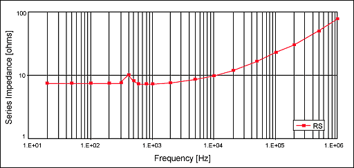
Figure 2. The impedance of a small 8Ω speaker remains 8Ω for most of the audio band, rising above 10Ω at 400Hz due to self resonance. Skin effect and voice-coil inductance yields higher resistance and reactance at higher frequencies, causing the impedance to rise above 10KHz and approach 100Ω at 1MHz.
For a particular speaker to be driven, you should verify the coil impedance at and above the switching frequency, and remember that excessively long speaker leads can add a parallel capacitive load that adversely affects the efficiency. The speaker leads and voice coil carry signals whose high dv / dt can radiate high levels of RF. Note that the switching action dissipates a small amount of power in the voice coil. Though negligible at 500KHz and above, it should be considered at lower frequencies when calculating the maximum permissible speaker power. Minimum Implementation with Resistive LoadsIf the load is mostly resistive, or looks capacitive at high frequencies, then other components must be added to ensure reasonable efficiency. A series inductor, for example, passes current to the load at audio frequencies but provides increasing impedance at higher frequencies.
As an example, consider an 8Ω resistive load driven by a MAX4295 amplifier from a 5V supply. In calculating the series inductor value we could simply assume that the 3dB roll-off point due to the inductor should be placed just outside the audio band, say at 30KHz: L = 8 / (2Πf) or 8 / 2Π(30 × 10³) = 42.4µH If we set a 250KHz switching frequency for our class D amplifier, the impedance seen by output devices at this point is due mostly to the inductor : XL = 2Π× 250 × 10³ × 42.4 × 10-6 = 66.7Ω, or more than 8X the load impedance, so no significant power is lost at the switching frequency.
We can now look at the other parameters that affect selection of the inductor. The data sheet tells us that the MAX4295 delivers 1.2W into 8Ω from a 5V supply. Thus, the inductor must handle about 387mArms (550mA peak) without saturation. Otherwise, the penalty is distortion in the output waveform.
We can therefore choose a 47µH SM power inductor from JW Miller Magnetics (model PM54-470L). Its rated current is 720mA (which handles the required peak current), and its DC resistance of 0.37Ω (less than 5% of the load) does not cause much efficiency loss. The inductor's physical dimensions are about 5.8mm x 5.2mm with a height of 4.5mm. (In contrast, the MAX4295 in a QSOP package measures only 6 x 5mm x 1.5mm.) That height can be unacceptably large for portable products, in which the space on and above the PCB is usually at a premium.
One way to reduce the profile of the inductor is to mount it in a hole or notch in the PCB. For a 1.6mm PCB, that approach reduces the inductor's height above the PCB to 2.9mm. Another approach is to increase the switching frequency of the class D stage. The MAX4295 / MAX4297 amplifiers allow the user to set this frequency to one of four values, the highest of which is 1MHz. Higher frequency allows lower inductance values, but the one-fourth value obtained from a 4 / X increase in frequency does not necessarily result in one quarter the physical size. Moreover, the thinner wire used in smaller-footprint inductors produces higher DC resistance, but some improvement should be possible.
Increasing the switching frequency by a factor of four in the previous example (from 250KHz to 1MHz) lets you reduce the inductor value by a factor of four (42.4µH / 4 = 10.6µH) while maintaining a constant impedance at the switching frequency. The required current handling and DC resistance are unchanged, however. Choosing to switch at 1MHz has little effect on efficiency, but it does degrade the THD + N performance slightly (see data sheet for details). Does it save board space? At 1MHz we can now use a 10µH inductor from Toko (model A914BYW-100M), with a current rating of 760mA and a DC resistance of 0.125Ω. XY dimensions are roughly the same, at 5mm x 5mm, but height above the PCB is only 2mm, without special mounting techniques. Compared with the 47µH inductor mentioned earlier, this component occupies only half as much volume. Output-Filter DesignThe above examples implement basic operation with a minimum of complexity, but rapid switching in the output devices provides little o r no filtering of the RF spectrum. Radiated from speaker leads and PCB traces, that energy can cause electro-magnetic interference (EMI). Controlling such unwanted EMI effects can be important for two reasons: The amplifier operates in a portable device, where other RF circuitry can be corrupted. The amplifier operates in a product subject to RF emissions standards testing (such as FCC / CE). Most applications require RF-suppression filtering on the outputs. For that purpose, the single inductor above can readily be turned into a lowpass filter by adding a capacitor to the complementary output (Figure 3). Radiation remains likely, however, because the speaker's OUT lead still sees the full switching-voltage waveform. A balanced 2-pole filter is therefore more effective (Figure 4) . EMI performance is much improved because the 2-pole filter provides low-pass filtering before the waveform reaches either speaker lead. Next, we consider the effect of these extra filter components on the PCB a rea.
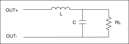
Figure 3. A conceptually simple, single-ended 2-pole LC filter is produced by adding capacitance to the inductor value specified by the equation for minimal implementation. Because the "OUT-" terminal is not filtered before the speaker, this filter does not reduce EMI sufficiently to meet regulatory requirements.
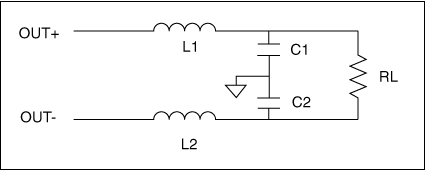
Figure 4. At the cost of additional components, a balanced 2-pole filter (the recommended approach) is effective in reducing EMI emissions. Each inductor value is half that of Figure 3. (See the text, and Figures 5 and 6.)
With two inductors now required, having a high impedance at the switching frequency for load and LP filter is still a benefit. Because the two inductors are effectively in series between the MOSFET outputs, we can halve the 10µH inductor values ​​and use two 5µH parts, while retaining the MAX4295's 1MHz switching frequency. From the Coilcraft catalog we can choose a 4.7µH inductor (model DT1608C-472) with a current rating of 1.2A and a DC resistance of 0.085Ω. Both specs are more than adequate for this application. Note that DC-resistance contributions are doubled because the inductors are in series with the load, giving a total of 0.17Ω. This value is only ~ 2% of the load resistance, so it has little effect on the efficiency.
The capacitance value can now be chosen to define the filter's high-frequency rolloff. Considering only one half of the differential output makes the math more straightforward, and allows us to realize a 2nd-order LCR filter in which R and L are known. Thus , we need only define the value of C (Figure 5). A ~ 4% voltage overshoot in response to a step input is acceptable, so the maximally flat Butterworth filter is a reasonable choice. Using math that is detailed elsewhere (see the Appendix and the MAX4295 data sheet), the value of C is
C = L / (4R²![]() ²) = 4.7x10⁻⁶ / (4 × 4² × (0.707) ²) = 0.146µF where
²) = 4.7x10⁻⁶ / (4 × 4² × (0.707) ²) = 0.146µF where ![]() equals 0.707 for Butterworth. This value can be realized with a network (called an% alternate balanced 2-pole filter% in the data sheet) of one capacitor across the inductors and one to ground from each output. Using three 0.047µF caps simplifies the bill of materials. Each + and à phase then sees a capacitance of 0.141µF (Figure 6). The filter's corner frequency is 192KHz. The inductors do not self-resonate below 60MHz, so the filter attenuates switching noise over a frequency span of two and a half decades (at that point the switching energy is falling rapidly anyway). Rise and fall times for the MAX4295 are about 30ns.
equals 0.707 for Butterworth. This value can be realized with a network (called an% alternate balanced 2-pole filter% in the data sheet) of one capacitor across the inductors and one to ground from each output. Using three 0.047µF caps simplifies the bill of materials. Each + and à phase then sees a capacitance of 0.141µF (Figure 6). The filter's corner frequency is 192KHz. The inductors do not self-resonate below 60MHz, so the filter attenuates switching noise over a frequency span of two and a half decades (at that point the switching energy is falling rapidly anyway). Rise and fall times for the MAX4295 are about 30ns.
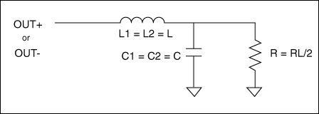
Figure 5. For analysis, a single-ended circuit that models the output seen by each half-circuit in Figure 4 can simplify the math somewhat.
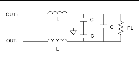
Figure 6. This 2-pole, differential-mode filter serves the example in the text. Inductor values ​​are 4.7µH, capacitor values ​​are 0.047µF, and the speaker impedance (RL) is 8Ω.
To minimize radiation, the PCB layout should place the inductors as close to the MAX4295 as possible. Tracking between the inductors and capacitors should also be minimized. The physical size (and cost) of the capacitors is much less of an issue than for the inductors . For the required 0.047µF capacitor, a 16V surface-mount, 0402 ceramic with X7R dielectric is available from AVX Corporation and others.
If filter optimization is important for the application, calculations should account for the high-frequency load impedance. Further accuracy can be gained by modelling the capacitor ESR, along with the inductors' DC resistance and self-resonant behavior. ResultsThe 2-pole filter of Figure 5 was tested with Coilcraft DT1608C-472 inductors, driving an 8Ω resistive load from one channel of a MAX4297 evaluation kit set with a 1MHz switching frequency. Efficiency was calculated with a 2V sine wave applied at four different frequencies:
Table 1. Measured Efficiency
These results show the high efficiency that class D devices can achieve, which is much higher than that of traditional class AB amplifiers. Figure 7 shows THD + N vs. frequency, measured over the 22Hz-22KHz bandwidth, with output power set to 0.7W at 1KHz. Distortion (THD + N) was measured at three different frequencies (1KHz, 5KHz, and 10KHz) while varying the output power, using an Audio Precision System One (Figure 8). The measurement bandwidth was 22Hz to 22KHz. The results shown are in broad agreement with the data sheet, with distortion dominating noise over most of the range. Distortion remains below 1% for all frequencies up to the 0.7W output-power level.
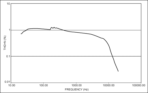
Figure 7. Operating at 1KHz with a power level of 0.7WRMS, a MAX4295 sensor with filter of Figure 6 exhibits distortion vs. frequency as shown. At that power level, the circuit delivers <or = 1% distortion over the entire band.
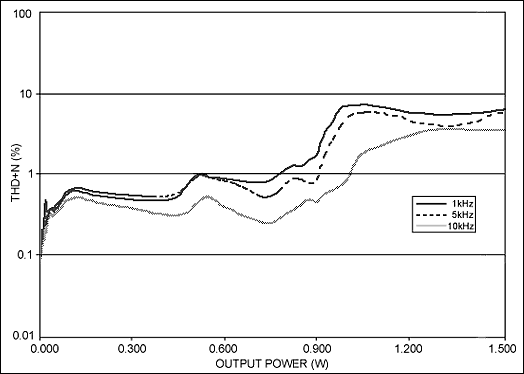
Figure 8. Distortion vs. output-power level for the MAX4295 sensor with filter of Figure 6 shows that distortion remains below 1% for power levels up to 0.7W, and rises sharply at 1W. (The solid line represents operation at 1KHz, the dashed line at 5KHz, and the grayed line at 10KHz.) SummaryBecoming familiar with the advantages and limitations of class D amplifiers and their design concepts allows the user to optimize any output filter for a given application. Informed design decisions can then be reached by weighing these often-conflicting requirements against one another: Appendix: 2nd-Order Filter Calculations The transfer function for the filter in Figure 5 can be expressed as: H (s) = (1 / LC) / (s² + s (1 / CR) + (1 / LC)) This H (s) expression can be equated to the generic 2nd-order system equation: G (s) = Ωn² / (s² + 2Ωn![]() s + Ωn²) R and L are known, so we can solve for C: C = L / (4R²
s + Ωn²) R and L are known, so we can solve for C: C = L / (4R² ![]() ²) The parameter Ωn is also useful:
²) The parameter Ωn is also useful:
Ωn = 1 / (√LC) rads-1 ___________________________
References and Further Reading MAX4295 / MAX4297 data sheet
Principles of Active Network Synthesis and Design, Gobind Daryanani (John Wiley & Sons, Inc.), 1976 Filter-Component Manufacturers Coilcraft
JW Miller Magnetics
Toko
AVX Corporation A similar version of this article appeared in the November 2001 issue of Electronik Industrie magazine.
|

The main advantage of class D amplifiers is their efficiency, which is higher than that of class AB amplifiers. As a minimum condition for achieving that efficiency, the load of a class D amplifier should present a high impedance at the switching frequency. In typical output waveforms (Figure 1) the duty cycle of the OUT + terminal varies but its pulse period is constant (the "ticks" shown between the two waveforms denote equal time periods). A running average of these pulses forms a slowly rising voltage (dashed line) over the sequence shown. Because the OUT- signal is the inverse of OUT +, it produces a slowly falling voltage. If the load is a speaker, in which the load is connected between the + and-terminals, this slow-moving component is audible but the high-frequency content is not reproduced.
Figure 1. These complementary PWM outputs are generated by a class D amplifier in the bridge configuration (like the MAX4295). The average values ​​of these waveforms (the dashed lines) are produced by an output filter, whose loss and distortion-producing artifacts should be held to a minimum.
Whether to use an output filter or not depends on many factors. Consider the following: the MAX4295 / MAX4297 audio power amplifiers contain complementary output MOSFETs that implement pulse-width modulation (PWM). The duty cycles for the output waveforms from these devices are approximately 50% with zero input signal applied, and to maintain reasonable efficiency the MOSFETs should drive a high impedance at the switching frequency. Otherwise, when a resistor is connected directly across the outputs with no other components present, the output stages conduct almost 100% of the time regardless of changes in the duty cycle.
Now consider the impedance plot of a speaker such as an 8Ω, 1.75 "cone transducer, for which the MAX4295 / MAX4297 amplifiers are suitable drivers (Figure 2). The speaker impedance rises beyond the audio band, but remains low below 20KHz. As implied earlier, the MAX4295 / MAX4297 output terminals are capable of driving this load directly. Indeed, the series inductance of the loudspeaker voice coil shown (approximately 10µH) allows efficient operation without a filter. That mode of operation has limitations, however.
Figure 2. The impedance of a small 8Ω speaker remains 8Ω for most of the audio band, rising above 10Ω at 400Hz due to self resonance. Skin effect and voice-coil inductance yields higher resistance and reactance at higher frequencies, causing the impedance to rise above 10KHz and approach 100Ω at 1MHz.
For a particular speaker to be driven, you should verify the coil impedance at and above the switching frequency, and remember that excessively long speaker leads can add a parallel capacitive load that adversely affects the efficiency. The speaker leads and voice coil carry signals whose high dv / dt can radiate high levels of RF. Note that the switching action dissipates a small amount of power in the voice coil. Though negligible at 500KHz and above, it should be considered at lower frequencies when calculating the maximum permissible speaker power. Minimum Implementation with Resistive LoadsIf the load is mostly resistive, or looks capacitive at high frequencies, then other components must be added to ensure reasonable efficiency. A series inductor, for example, passes current to the load at audio frequencies but provides increasing impedance at higher frequencies.
As an example, consider an 8Ω resistive load driven by a MAX4295 amplifier from a 5V supply. In calculating the series inductor value we could simply assume that the 3dB roll-off point due to the inductor should be placed just outside the audio band, say at 30KHz: L = 8 / (2Πf) or 8 / 2Π(30 × 10³) = 42.4µH If we set a 250KHz switching frequency for our class D amplifier, the impedance seen by output devices at this point is due mostly to the inductor : XL = 2Π× 250 × 10³ × 42.4 × 10-6 = 66.7Ω, or more than 8X the load impedance, so no significant power is lost at the switching frequency.
We can now look at the other parameters that affect selection of the inductor. The data sheet tells us that the MAX4295 delivers 1.2W into 8Ω from a 5V supply. Thus, the inductor must handle about 387mArms (550mA peak) without saturation. Otherwise, the penalty is distortion in the output waveform.
We can therefore choose a 47µH SM power inductor from JW Miller Magnetics (model PM54-470L). Its rated current is 720mA (which handles the required peak current), and its DC resistance of 0.37Ω (less than 5% of the load) does not cause much efficiency loss. The inductor's physical dimensions are about 5.8mm x 5.2mm with a height of 4.5mm. (In contrast, the MAX4295 in a QSOP package measures only 6 x 5mm x 1.5mm.) That height can be unacceptably large for portable products, in which the space on and above the PCB is usually at a premium.
One way to reduce the profile of the inductor is to mount it in a hole or notch in the PCB. For a 1.6mm PCB, that approach reduces the inductor's height above the PCB to 2.9mm. Another approach is to increase the switching frequency of the class D stage. The MAX4295 / MAX4297 amplifiers allow the user to set this frequency to one of four values, the highest of which is 1MHz. Higher frequency allows lower inductance values, but the one-fourth value obtained from a 4 / X increase in frequency does not necessarily result in one quarter the physical size. Moreover, the thinner wire used in smaller-footprint inductors produces higher DC resistance, but some improvement should be possible.
Increasing the switching frequency by a factor of four in the previous example (from 250KHz to 1MHz) lets you reduce the inductor value by a factor of four (42.4µH / 4 = 10.6µH) while maintaining a constant impedance at the switching frequency. The required current handling and DC resistance are unchanged, however. Choosing to switch at 1MHz has little effect on efficiency, but it does degrade the THD + N performance slightly (see data sheet for details). Does it save board space? At 1MHz we can now use a 10µH inductor from Toko (model A914BYW-100M), with a current rating of 760mA and a DC resistance of 0.125Ω. XY dimensions are roughly the same, at 5mm x 5mm, but height above the PCB is only 2mm, without special mounting techniques. Compared with the 47µH inductor mentioned earlier, this component occupies only half as much volume. Output-Filter DesignThe above examples implement basic operation with a minimum of complexity, but rapid switching in the output devices provides little o r no filtering of the RF spectrum. Radiated from speaker leads and PCB traces, that energy can cause electro-magnetic interference (EMI). Controlling such unwanted EMI effects can be important for two reasons: The amplifier operates in a portable device, where other RF circuitry can be corrupted. The amplifier operates in a product subject to RF emissions standards testing (such as FCC / CE). Most applications require RF-suppression filtering on the outputs. For that purpose, the single inductor above can readily be turned into a lowpass filter by adding a capacitor to the complementary output (Figure 3). Radiation remains likely, however, because the speaker's OUT lead still sees the full switching-voltage waveform. A balanced 2-pole filter is therefore more effective (Figure 4) . EMI performance is much improved because the 2-pole filter provides low-pass filtering before the waveform reaches either speaker lead. Next, we consider the effect of these extra filter components on the PCB a rea.
Figure 3. A conceptually simple, single-ended 2-pole LC filter is produced by adding capacitance to the inductor value specified by the equation for minimal implementation. Because the "OUT-" terminal is not filtered before the speaker, this filter does not reduce EMI sufficiently to meet regulatory requirements.
Figure 4. At the cost of additional components, a balanced 2-pole filter (the recommended approach) is effective in reducing EMI emissions. Each inductor value is half that of Figure 3. (See the text, and Figures 5 and 6.)
With two inductors now required, having a high impedance at the switching frequency for load and LP filter is still a benefit. Because the two inductors are effectively in series between the MOSFET outputs, we can halve the 10µH inductor values ​​and use two 5µH parts, while retaining the MAX4295's 1MHz switching frequency. From the Coilcraft catalog we can choose a 4.7µH inductor (model DT1608C-472) with a current rating of 1.2A and a DC resistance of 0.085Ω. Both specs are more than adequate for this application. Note that DC-resistance contributions are doubled because the inductors are in series with the load, giving a total of 0.17Ω. This value is only ~ 2% of the load resistance, so it has little effect on the efficiency.
The capacitance value can now be chosen to define the filter's high-frequency rolloff. Considering only one half of the differential output makes the math more straightforward, and allows us to realize a 2nd-order LCR filter in which R and L are known. Thus , we need only define the value of C (Figure 5). A ~ 4% voltage overshoot in response to a step input is acceptable, so the maximally flat Butterworth filter is a reasonable choice. Using math that is detailed elsewhere (see the Appendix and the MAX4295 data sheet), the value of C is
C = L / (4R²
Figure 5. For analysis, a single-ended circuit that models the output seen by each half-circuit in Figure 4 can simplify the math somewhat.
Figure 6. This 2-pole, differential-mode filter serves the example in the text. Inductor values ​​are 4.7µH, capacitor values ​​are 0.047µF, and the speaker impedance (RL) is 8Ω.
To minimize radiation, the PCB layout should place the inductors as close to the MAX4295 as possible. Tracking between the inductors and capacitors should also be minimized. The physical size (and cost) of the capacitors is much less of an issue than for the inductors . For the required 0.047µF capacitor, a 16V surface-mount, 0402 ceramic with X7R dielectric is available from AVX Corporation and others.
If filter optimization is important for the application, calculations should account for the high-frequency load impedance. Further accuracy can be gained by modelling the capacitor ESR, along with the inductors' DC resistance and self-resonant behavior. ResultsThe 2-pole filter of Figure 5 was tested with Coilcraft DT1608C-472 inductors, driving an 8Ω resistive load from one channel of a MAX4297 evaluation kit set with a 1MHz switching frequency. Efficiency was calculated with a 2V sine wave applied at four different frequencies:
Table 1. Measured Efficiency
| Input Frequency (KHz) | Efficiency (%) |
1 | 74.9 |
5 | 84.3 |
10 | 86.3 |
15 | 86.7 |
These results show the high efficiency that class D devices can achieve, which is much higher than that of traditional class AB amplifiers. Figure 7 shows THD + N vs. frequency, measured over the 22Hz-22KHz bandwidth, with output power set to 0.7W at 1KHz. Distortion (THD + N) was measured at three different frequencies (1KHz, 5KHz, and 10KHz) while varying the output power, using an Audio Precision System One (Figure 8). The measurement bandwidth was 22Hz to 22KHz. The results shown are in broad agreement with the data sheet, with distortion dominating noise over most of the range. Distortion remains below 1% for all frequencies up to the 0.7W output-power level.
Figure 7. Operating at 1KHz with a power level of 0.7WRMS, a MAX4295 sensor with filter of Figure 6 exhibits distortion vs. frequency as shown. At that power level, the circuit delivers <or = 1% distortion over the entire band.
Figure 8. Distortion vs. output-power level for the MAX4295 sensor with filter of Figure 6 shows that distortion remains below 1% for power levels up to 0.7W, and rises sharply at 1W. (The solid line represents operation at 1KHz, the dashed line at 5KHz, and the grayed line at 10KHz.) SummaryBecoming familiar with the advantages and limitations of class D amplifiers and their design concepts allows the user to optimize any output filter for a given application. Informed design decisions can then be reached by weighing these often-conflicting requirements against one another: Appendix: 2nd-Order Filter Calculations The transfer function for the filter in Figure 5 can be expressed as: H (s) = (1 / LC) / (s² + s (1 / CR) + (1 / LC)) This H (s) expression can be equated to the generic 2nd-order system equation: G (s) = Ωn² / (s² + 2Ωn
Ωn = 1 / (√LC) rads-1 ___________________________
References and Further Reading MAX4295 / MAX4297 data sheet
Principles of Active Network Synthesis and Design, Gobind Daryanani (John Wiley & Sons, Inc.), 1976 Filter-Component Manufacturers Coilcraft
JW Miller Magnetics
Toko
AVX Corporation A similar version of this article appeared in the November 2001 issue of Electronik Industrie magazine.
Smart Ceiling Fan,Intelligence Ceiling Fan,Five Blades Ceiling Fan,5 Blades Ceiling Fan
Jiangmen MagicPower Electrical Appliances Co.,Ltd. , https://www.magicpowerfan.com