802.11b WLAN low noise amplifier—MAX2644 meeting 10µs switching time
Abstract: This application note gives the measurement of the startup and shutdown time of the MAX2644 low noise amplifier (LNA), which is necessary to support IEEE® 802.11b TDD WLAN systems. The system works at 2.4GHz with a startup time of 8.6µs and a shutdown time of 5µs. The test results of oscilloscope and vector signal analyzer are given.
There are many types of IEEE 802.11b wireless local area network (WLAN) network cards currently on the market. These WLAN network cards operating in the open 2.4GHz band are becoming increasingly popular in office and home applications, and they can provide variable rate data transmission up to 11Mbps. Perhaps a very important parameter that distinguishes a network card from other competing products is the operating range, which can also be said to be the sensitivity of the receiver.
The superheterodyne receiver is the most adopted solution for WLAN network cards on the market today. As the next generation of WLAN network cards require lower bill of materials (BOM) costs, direct conversion receivers are becoming more and more popular because they do not require expensive intermediate frequency filters and are replaced with on-chip integrated low-pass filters Select a channel. According to the actually selected receiver architecture and working process, a low-noise amplifier (LNA) is needed to effectively reduce the noise figure of the entire system, thereby improving the working range of the receiver.
The MAX2644 is based on low-noise, advanced silicon germanium (SiGe) technology and is an excellent choice for 2.4GHz WLAN applications. This low-cost, high-IP3 LNA has an adjustable bias feature, allowing input IP3 and source current to be optimized for specific applications. The LNA has an input IP3 of + 1dBm and can maintain a low noise figure of 2.0dB and a typical gain of 16dB.
Because IEEE 802.11b is a time division multiplexing (TDD) system, LNA must have a fast "on-off" capability to meet the requirements of the system. Generally, 10µs is an acceptable limit. Tests in the laboratory show that the turn-on time of the MAX2644 is approximately 8.6µs (the output power is increased from -30dBm to -13dBm ± 1dB). The turn-off time for a 30dB drop from the rated output power is 5µs. Both times meet the requirement of 10µs.
Table 1. MAX2644 switching time characteristics
| Settling TIme | Test CondiTIon | |
| Turn-on TIme | 8.6µs | Output power settles to within ± 1dB. |
| Turn-off TIme | 5µs | Power level drops to -30dBc from nominal output power level. |
Testing process
Prepare a standard MAX2644 evaluation board, and add ROHM® low-power NPN digital transistor (DTC144) to the bias network to implement shutdown control, as shown in Figure 1. The logic high level of the transistor is 2.7Vdc, indicating conduction. An equivalent field effect transistor (FET) switch can also be used here. 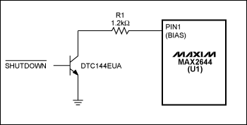
Figure 1. Modify the standard evaluation board
See Figure 2 for all tested devices. 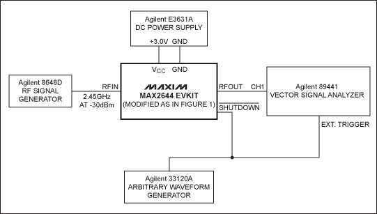
Figure 2. MAX2644 switching time test device
In burst mode, an arbitrary waveform generator can be selected to generate TTL compatible 2.8VPEAK logic pulses with a pulse width of 62.5µs, as shown in Figure 3. 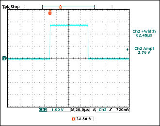
Figure 3. Trigger pulse applied to DTC144EUA digital transistor
The trigger pulse is sent to the transistor marked / shutdown on the evaluation board, and also to the external vector signal analyzer. This method makes the starting point of the switching pulse and measurement data consistent.
The vector signal analyzer is configured to display power (dBm, 1MHz bandwidth) and time, and the time scale is the same as the time scale of the trigger pulse. The test results using this method are shown in Figure 4 and Figure 5. Note that the X-axis (time) directly refers to the time axis that turns on the MAX2644 trigger pulse without any delay. The "off" trigger pulse in the figure occurs after 62.5 µs. 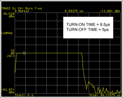
Figure 4. Output power and time (10dB / div) 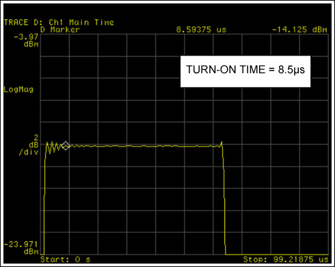
Figure 5. Output power and time (2dB / div)
Bi Directions Thyristor (Triac) is equivalent to the antiparallel connection of two unidirectional thyristors, but only one control pole.
Bidirectional thyristors are made of N-P-N-P-N five-layer semiconductor materials, and three electrodes are also derived from the outside. Its structure is shown in the figure. Bi-directional thyristor volt-ampere characteristic curve Since the forward and reverse characteristics of the bidirectional thyristor are symmetrical, it can be turned on in any direction and is an ideal AC switching device.
Bi Directions Thyristor (Triac)
Bi Directions Thyristor,Electronic Components Triac,Power Thyristor For Inverter,Silicon Power Bipolar Transistors
YANGZHOU POSITIONING TECH CO., LTD. , https://www.yzpst.com