In addition to structural simplification, rare earth high-power LED lamps integrate the following technologies: heat sink and lamp housing integrated heat dissipation structure, monolithic structure, so that the lamps are completely exposed in the ambient air, no regenerative cavity exists; rare earth alloy material production The heat conductivity of the radiator is high and the thermal resistance is low. The structure of the rare earth alloy uniform temperature plate makes the heat dissipation uniform and has no high temperature region; the precision matching technology between different heat conductive materials and the thermal deformation modulus matching technology make the contact tight and the thermal resistance is low; The use of high-efficiency heat-conducting dielectric materials reduces the thermal resistance of the contact surface; the aerodynamic and thermodynamic principles are used to design a perforated three-dimensional grid-like heat sink to form a “chimney-type†heat dissipation method to accelerate the air convection cycle, and the through-hole structure makes the dust have nowhere to be attached. The direct contact area between the heat sink and the air is ensured; the nano-thermal radiation coating increases the heat radiation capability of the lamp.
The continuous improvement of rare earth phosphors has benefited the overall lighting industry - metal halide lamps, high pressure sodium lamps, fluorescent tube energy-saving lamps and the latest high-power LED lamps.
High-efficiency light source conversion enables high-power LED lamps to improve light efficiency and reduce heat consumption. The same power consumption can have higher brightness; if the brightness is equal, it is equal to the heat loss. This is naturally beneficial for LED chips that are afraid of heat. However, since the energy that is actually converted into light energy to emit the illuminant is only about 30%, most of the energy remains in the form of heat on the LED chip.
The substrate material and solid crystal mode of the LED chip itself are becoming more and more efficient and heat conduction:
1. US CREE's unique silicon carbide substrate is the highest thermal conductivity LED chip substrate. The 40x40mil chip can withstand 1000MA current. As long as the subsequent heat dissipation does not have this rated 1W power chip, 3W is used. There are no concerns about burning.
2. The chip of the traditional sapphire substrate, not showing weakness, developed a method of flip chip mounting chip. The two electrodes on the surface are turned to the bottom surface and directly soldered to the metal heat conductive substrate with silver paste. This heat transfer is more straightforward than the conventional use of thermally conductive silver paste. In addition, high-power LED chips from recent days, South Korea and Taiwan also have a method of adding a metal plating layer on the sapphire substrate, so that silver paste can be used instead of silver glue to solidify the crystal. After the silver paste is cured, the thermal conductivity is close to that of pure silver, which is higher than the thermal conductivity of the silver paste.
Improvement of Thermal Conductive Copper Sheet--Diamond-Copper Composite
If the LED chip is not directly bonded to the circuit substrate by COB, a material with fast heat conduction is used as an intermediate medium for connecting the heat sink fins. Copper is a material that is only slightly inferior to silver in metal, and its price is lower, so copper is currently the most common thermal transfer material for high-power LED chips.
However, the coefficient of thermal expansion of copper (about 19) is much larger than the coefficient of thermal expansion of the sapphire substrate (about 5). Therefore, the use of copper as a chip thermal carrier in the harsh environment, there is a risk of chip chipping. The chip size is limited. Nowadays, diamond-copper composite sheets have been developed in China. The thermal conductivity is higher than that of pure copper; the thermal expansion coefficient is lower than that of copper. It is expected that after mass production, the price can be accepted by manufacturers that produce high-power LED chip integrated blocks. The latest experimental report, using a 100W integrated module comparison, with a pure copper module at a chip temperature of 75 degrees Celsius, the module temperature of the diamond-copper composite chip is only 65 degrees Celsius.
From the improvement of the luminous efficacy of rare earth phosphors to the improvement of chip solid crystal and the breakthrough of thermal conductive sheet materials, 2010 is a symbol year. High-power LED lighting will be closer to our lives!
PCB Prototype
Prototype PCB Specification:
In the process of developing a Printed Circuit Board-based solution for your company? This can be an extremely time-consuming, labor-intensive process where there is a high degree of uncertainty in the outcome. Developing a PCB prototype offers a fast, cost-effective option for getting your design from concept to production, while minimizing some of the risks associated with a Standard PCB service.
Prototype Printed Circuit Boards That Meet Our High Quality Standards:
BentePCB offers rapid PCB prototyping services in very good quality yet at a low cost. We're fully compliant with ISO9001:2008 quality management systems, and we have an in-house quality control department to verify that all work meets our high standards. Depending on your custom requirements, we can prototype your PCB within 3-7 days, compared to -18 days of Standard PCB service.
Check out our Circuit Board prototype capabilities in the following table:
|
Features |
Capability |
|
Quality Grade |
Standard IPC 2 |
|
Number of Layers |
1 - 16layers |
|
Order Quantity |
5pcs - 100pcs |
|
Build Time |
2 - 7 days |
|
Material |
FR-4 Standard Tg 140°C |
|
Board Size |
Min 6*6mm | Max 500*500mm |
|
Board size tolerance |
±0.1mm - ±0.3mm |
|
Board Thickness |
0.4mm - 2.0mm |
|
Board Thickness Tolerance |
±0.1mm - ±10% of thickness of board |
|
Copper Weight |
1.0oz - 2.0oz |
|
Inner Layer Copper Weight |
0.5oz - 1.0oz |
|
Copper Thickness Tolerance |
+0μm +20μm |
|
Min Tracing/Spacing |
5mil/5mil |
|
Solder Mask Sides |
As per the file |
|
Solder Mask Color |
Green, White, Blue, Black, Red, Yellow |
|
Silkscreen Sides |
As per the file |
|
Silkscreen Color |
White, Black |
|
Surface Finish |
Lead
Free HASL - RoHS |
|
Min Annular Ring |
5mil |
|
Min Drilling Hole Diameter |
8mil |
|
Min Width of Cutout (NPTH) |
0.8mm |
|
NPTH Hole Size Tolerance |
±.002" (±0.05mm) |
|
Min Width of Slot Hole (PTH) |
0.6mm |
|
PTH Hole Size Tolerance |
±.003" (±0.08mm) - ±.006" (±0.15mm) |
|
Surface/Hole Plating Thickness |
20μm - 30μm |
|
SM Tolerance (LPI) |
.003" (0.075mm) |
|
Aspect Ratio |
1.10 (hole size: board thickness) |
|
Test |
10V - 250V, flying probe or testing fixture |
What Are the Benefits of Circuit Board Prototyping?
We recommend you chose PCB prototyping service for function testing of new products prior to making a commitment to a full-production run. Benefits of developing PCB board prototype include:
• Rapidly test and correct designs if there is any mistake
• Opportunity to detect potential design flaws in the early stages
• Quick turnaround time helps you achieve your productivity goals
• Low-quantity production runs featuring a minimum order quantity of only one boards
• Lower production tolerances provide a clear indication of how well the finished PCB will perform
Once your prototype boards demonstrated their ability to meet your quality and performance requirements, it is ready for a full production run. Then we will transition to Standard PCB service. It provides tighter production tolerances and more advanced options including free Design for Manufacture (DFM) check that is capable of detecting potential issues which could reduce the quality of your PCB.
About Us:
BentePCB is a professional PCB manufacturing which is focus on double side, multilayer, HDI PCB , rigid PCB and Flexible PCB mass production. The company was established on 2011.
We have two factories together, The factory in Shenzhen is specialized in small and middle volume orders and the factory in Jiangxi is for big volumn.
Why Us?
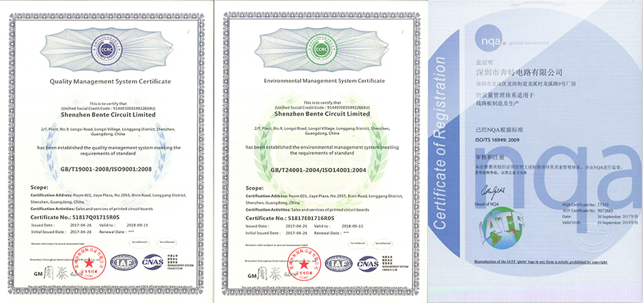
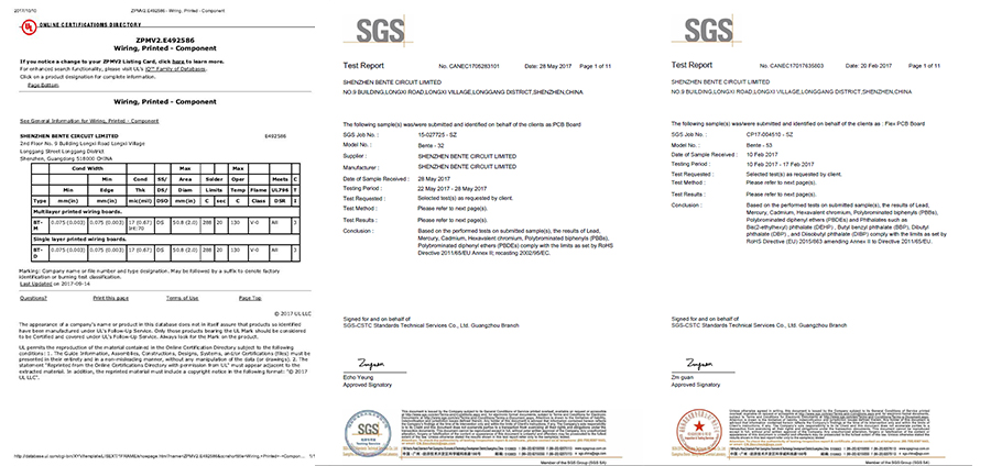
UL (E492586), ISO9001, ISO14001, TS16949, RoHS certified.
Turnover USD 10-50 million per year.
15,000 sqm area, 450 staff .
Mass Production from single to 16 layers.
Special Material:ROGERS, Arlon, Taconic.etc.
Client:Huawei, SAMSUNG, Malata, Midea,Texas Instruments.etc.
Certification(UL:E492586, TS16949, ISO14001, ISO9001,RoHS):
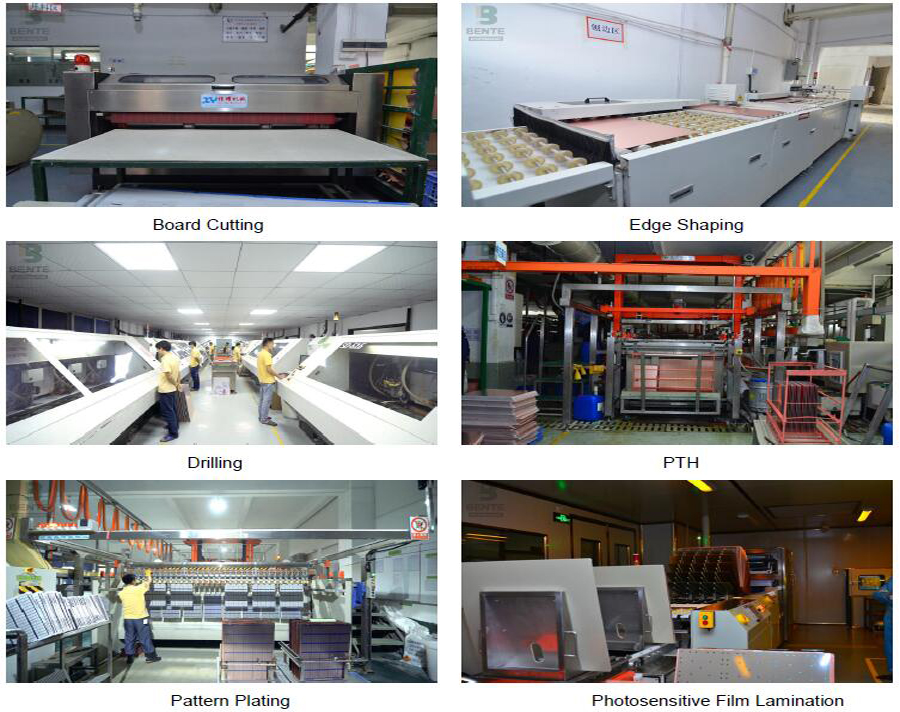
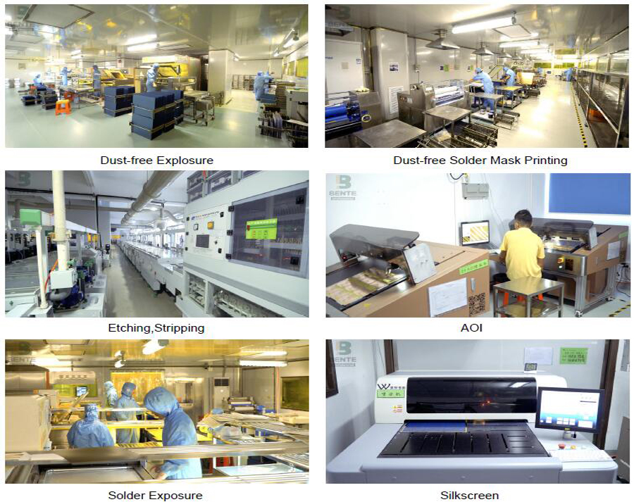
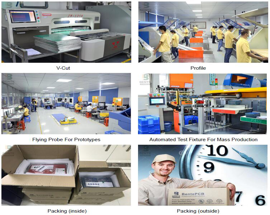
Factory Tour:
Exhibition:
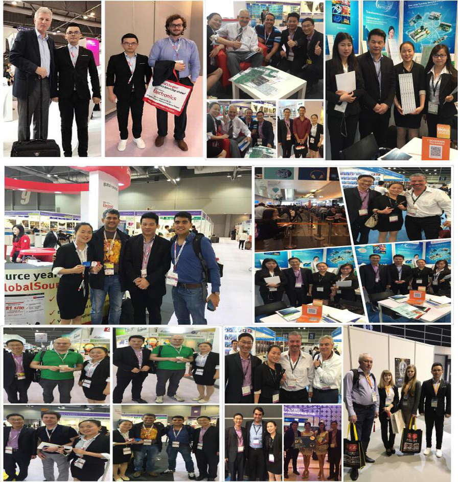
We Took part in the famous exhibitions over the past years,and got highly appreciation from the top experts,as well as cooperated tightly with them.
Delivery:
BentePCB offers flexible shipping methods for our customers, you may choose from one of the methods below.

FAQ:
Q1: What does BentePCB need for a customized PCB order?
A: The customers need to provide Gerber or pcb file.If you do not have the file in the correct format, you can send all the details related to the products.
Q2: What is your quotation policy?
A: For the PCB order in large quantity, BentePCB will send you the quotation based on the MOQ of the products concerned, and the price will be reasonable with good quality.
Q3: How long will you send us quotation ?
A: After all files were sent, 2 to 8 hours as per your file.
Q4:What is your minimum order quantity?
A:Our MOQ is 1 PCS.
Q5: How about the service BentePCB offered to the customers?
A: If you have any questions about our products or company, do not hesitate to send us your inquiry toour customer service representatives, Your satisfaction is our pursuits.

We don`t just sell PCBs .We sell sleep.

Prototype PCB
Prototype PCB, Prototype PCB Board, Prototype Printed Circuit Board, High Density Prototype PCB
Shenzhen Bente Circuit Limited , http://www.bentegroup.com