Users are demanding smaller, more affordable phones that offer faster service and enhanced features in handheld devices. This growing demand is pushing the industry to accelerate innovation and reduce costs in order to bring products to market quickly. As a result, manufacturers are reevaluating their technologies to meet these challenges effectively.
Silicon-based technology and integrated key components, such as RF transceivers, have significantly reduced both the size and cost of mobile devices. However, the strict performance requirements of cellular standards like GSM previously limited the integration of RF transceivers, leading to the use of alternative technologies such as SiGe BiCMOS or bipolar. With the increasing popularity of GSM/GPRS CMOS transceivers, the choice of CMOS for RF design has become more mature and reliable.
Despite the clear advantages of CMOS RF transceiver designs, engineers face several challenges when developing highly integrated multimode transceivers that support WCDMA, EDGE, GPRS, and GSM standards. Nevertheless, investing time and effort into CMOS-based RF transceivers for multimode applications is proving worthwhile, as the market response has been positive.
**The Multi-Mode Development Trend**
To meet the needs of global operators and different cellular architectures, handset manufacturers are integrating multiple wireless technologies into a single device. This approach allows them to offer the best solution for specific markets. For example, the number of handsets supporting EDGE has increased, and they remain backward compatible with GSM/GPRS services. Looking ahead, 3G phones will also support WCDMA alongside existing technologies like EDGE, GPRS, and GSM. Global roaming requires coverage across five frequency bands: GSM-850MHz, E-GSM-900MHz, DCS-1800MHz, PCS-1900MHz, and UMTS-2100MHz. Designers must address all these requirements while keeping costs low and form factors compact.
Silicon and module integration play a crucial role in enabling multi-mode functionality. Most multimode platforms combine separate wireless subsystems. For instance, a phone supporting both GSM/GPRS and WCDMA may have a WCDMA transceiver along with a GSM/GPRS transceiver, plus an RF front-end and passive components to handle two modes and bands. This method is practical because the reference clock frequencies for GSM/GPRS (13MHz/26MHz) and WCDMA (19.2MHz) differ. A typical GSM/GPRS transmitter structure, such as OPLL, cannot be directly used for WCDMA. Therefore, higher levels of integration and innovative RF technology are necessary to reduce component count and overall costs.
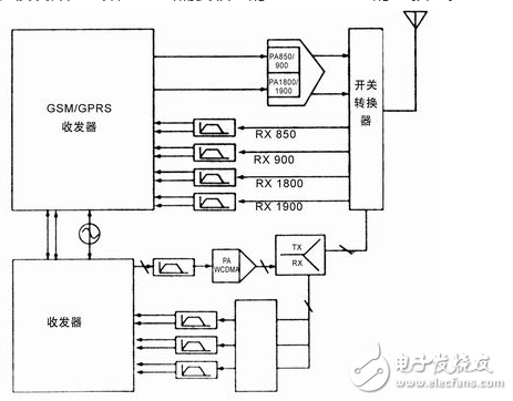
*Figure 1. Typical 3G multimode/multiband RF design with separate 3G and 2G wireless technologies*
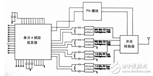
*Figure 2: Block diagram of a single 4-band GSM/GPRS CMOS transceiver*
**Multi-RF Front-End System Integration Solution**
The RF front-end design for a 4-band GSM/GPRS system is shown in Figure 2, using a highly integrated single-chip CMOS transceiver. The antenna switch module connects to the transmit and receive paths, and each GSM band uses a receiver SAW filter and matching circuitry. The transmit path requires at least two power amplifiers (PAs): one for the GSM-850MHz and E-GSM-900MHz bands, and another for the 1.8GHz DCS and 1.9GHz bands.
Many integrated RF front-end modules help reduce the number of components and simplify the design. These include PA modules with power control logic and transmitter modules that integrate PA and switching functions. On the receiving side, the system includes a SAW filter unit and an RF front-end module with a multiplexer and a receive filter.
Compared to the GSM/GPRS system in Figure 2, the more complex front-end design of the 3G multimode system in Figure 1 supports both 2.5G and 3G RF signal transmission. Adding a multiplexer is essential due to WCDMA’s frequency division duplexing, which requires simultaneous switching between transmitter and receiver. However, economic scaling continues to drive front-end component integration.
Today’s cellular base station architectures fall into two main categories: either splitting baseband functions into discrete analog and digital baseband chips or using monolithic, highly integrated CMOS SoC devices that include both mode implementation and digital functions. Choosing between these approaches depends on factors like future integration strategies and economic feasibility.
While the monolithic approach saves PCB space, using separate analog and digital baseband chips is often preferred for integration. This approach isolates analog baseband functionality from the “pure†digital circuits that implement the digital baseband. A two-chip solution also allows the digital baseband to scale to smaller CMOS geometries while integrating other components like application processors, image processors, and memory.
A growing trend in baseband architecture is to eliminate the analog baseband chip entirely, optimizing digital baseband functionality and simplifying the interface between wireless and baseband chips. This method uses a high-speed digital interface between the wireless and digital baseband, which can be either serial or parallel. While a serial interface reduces pin count, it increases transistor count on the chip. A parallel interface, though requiring more pins and a larger package, is more silicon-efficient.
The DigRF Standards Body now specifies a standard high-speed serial interface for 2.5G systems (see Figure 3). Supporting digital interfaces adds complexity to wireless design, as it requires not only analog-to-digital and digital-to-analog conversions but also interface logic for handling baseband communications. These functions are easier and more cost-effective to implement using CMOS technology.
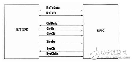
*Figure 3: 2G DigRF interface between wireless and digital baseband*
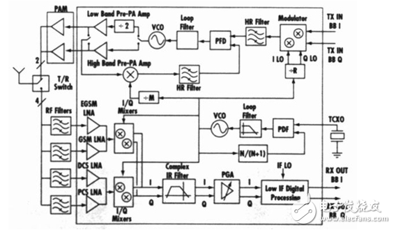
*Figure 4: Single-chip 4-band CMOS transceiver block diagram*
**Advantages of CMOS**
Implementing transceivers in CMOS technology offers several benefits:
- CMOS has a lower wafer cost compared to SiGe BiCMOS at similar process sizes.
- It allows fabrication in multiple foundries using standard processes.
- According to Moore’s Law, CMOS designs can scale to smaller process nodes.
- CMOS enables RF-enabled digital circuits, offering a highly programmable design that results in small chips, high manufacturability, and robust performance.
- CMOS transceivers can integrate additional functions, such as DigRF interfaces or digital baseband functionality, into a single RF and baseband component.
- CMOS has proven effective in implementing transceivers, with many manufacturers producing numerous GSM/GPRS, WLAN, and Bluetooth radios.
- The choice of transceiver architecture for multimode GSM/GPRS/EDGE/WCDMA handsets is critical. High integration in monolithic CMOS transceivers typically includes VCOs, frequency synthesizers, loop filters, and DCXO. This level of integration ensures better wireless performance by shielding critical functions from external noise sources.
Fiber Optic Patch Panel,Fiber Patch Panel,Fiber Distribution Panel,Optical Patch Panel
Cixi Dani Plastic Products Co.,Ltd , https://www.danifiberoptic.com