In Application Programming (IAP) in an FPGA can be implemented in two main ways. The first approach involves adding external circuitry to the board, such as using an MCU or CPLD to receive configuration data and program the FPGA in a passive serial (PS) mode. This method typically involves programming an external Flash device (like EPCS or other Flash chips) and then resetting the FPGA via its configuration pin. The FPGA then self-configures using the master string mode. The second method uses an internal CPU, such as Nios II, or a dedicated IP core within the FPGA to receive programming data, store it in a Flash chip, and then reset the FPGA through a simple external circuit to configure it in active serial (AS) mode.
To reduce board space, lower costs, and improve system reliability, this design utilizes the second method. The key requirements for the system include: hardware configured in AS mode (MSEL[1:0] set to 1:0), support for EPCS or both EPCS and Flash, and the ability to communicate with a PC. The FPGA receives update data, stores it in the Flash, and then resets either the Nios II or the FPGA itself to perform the update.
**1. System Hardware Design**
The system consists of a Cyclone FPGA, an EPCS chip, a Flash memory, and a serial communication interface. The hardware architecture is illustrated in Figure 1.
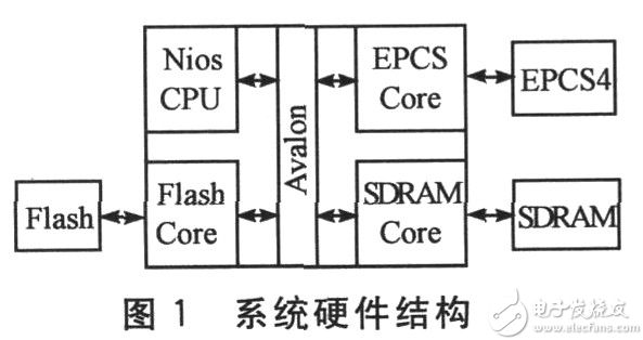
EPCS4 from Altera is used, which has a 4 Mb capacity, fewer pins, and supports 3.3 V low-voltage operation. For larger storage needs, an AMD Am29LV640MH/L Flash chip is used, offering 64 Mb of capacity, 3.0 V operation, low power consumption, and compatibility with the Cyclone FPGA. It also supports the CFI_FLASH core for SOPC design, making it easier to implement the hardware circuit.
**2. Working Principle**
**2.1 Key Concepts**
- **FPGA Configuration Data**: This refers to the .sof file, which is programmed into the Flash. Upon power-up, the FPGA reads the configuration data from the Flash.
- **Software Data**: Generated via the Nios II IDE as an .elf file, this data is stored in the Flash and loaded into the Nios II CPU after a reset.
**2.2 Programming Files**
Programming files are typically in S-Record (SREC) format, a standard developed by Motorola. Each line starts with 'S', followed by a record type, byte count, address, data bytes, and a checksum. This format ensures reliable data transmission during programming.
**2.3 AS Configuration Mode**
In AS mode, the FPGA reads configuration data from the EPCS and loads it into its internal SRAM. This mode is supported by Cyclone and Stratix II FPGAs. MSEL[1:0] must be set to 1:0 to enable AS mode. During configuration, the FPGA acts as the master, while the EPCS acts as the slave. Data is transferred via DCLK and DATA0, with configuration signals like nCONFIG, nSTATUS, and CONF_DONE managing the process.
**3. Workflow**
**3.1 Hardware Configuration Update**
The FPGA configuration process includes three main stages: reset, configuration, and initialization.
- **(1) Reset FPGA**: Upon power-on, if nCONFIG is held low for 40 μs, the FPGA enters reset. It samples MSEL to determine the configuration mode and initializes internal registers.
- **(2) Configure FPGA**: After reset, nCONFIG is pulled high, and the FPGA begins loading configuration data from the EPCS. The configuration process is controlled by nCS0, DCLK, and ASDO.
- **(3) Initialization Phase**: The FPGA uses an internal 10 MHz clock or CLKUSR for initialization. Once complete, the FPGA enters user mode.
- **(4) User Mode**: In this mode, I/O pins are configured according to the design. The FPGA can be reconfigured by pulling nCONFIG low again.
- **(5) Error Handling**: If a configuration error occurs, the FPGA sets nSTATUS and CONF_DONE low. With Auto-restart enabled, it attempts to reconfigure automatically; otherwise, the system must handle the error manually.
The computer communicates with the Nios II program on the target board, transfers the Flash file, and stores the data in SDRAM before writing it to EPCS or Flash. This prevents data loss in case of transfer failure.
To generate a Flash file, use the `sof2Flash` command in the Nios II command shell. The generated Flash file is stored in the project directory or under the Nios II example folder.
Computer Case, Desktop Computer Case, Console Case,Gaming Computer Case,Boluo Xurong Electronics Co., Ltd.
Boluo Xurong Electronics Co., Ltd. , https://www.greenleaf-pc.com