Wireless power supply is an attractive production topic. Many electronic magazines and forums have introduced the introduction of wireless power supply circuits. Although these circuits have their own advantages, they all have a common shortcoming. First, the transmission efficiency is not ideal. Second, regardless of the presence or absence of the receiver, the transmitting part continues to emit energy continuously as it is, which is unsatisfactory.
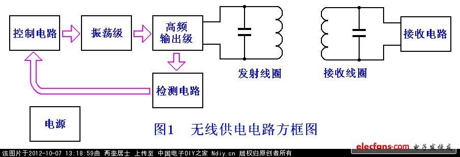
The wireless power supply device designed by the author, in addition to the high transmission efficiency, has a remarkable feature: it can automatically detect the presence or absence of the receiving part of the work, and only when it detects that the receiver is working, it will continuously radiate the radio energy. Otherwise, it will always work only in the low-energy detection state. Its working block diagram is shown in Figure 1:
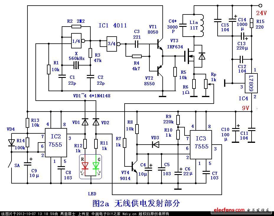
The combination of the CMOS circuit and the FET is used in the transmitting part. This combination is not only efficient but also easy to control. The transmitting coil adopts a Litz wire and a spider wire winding method to achieve higher conversion efficiency. The circuit is shown in Figure 2a:
Working principle :
Emission section
The oscillation source consists of a quarter crystal CD4011 and a crystal for the remote control. The measured oscillation frequency is 560 kHz. This frequency has two interferences in the middle band of the radio: 560 kHz and 1120 kHz. Because there is no more suitable crystal choice at hand, I have to do it.
4011 is a 2-input NAND gate, so whether the circuit works or not depends on the potential of the other input. The potential of this input is determined by the state of IC2 (555 circuit). The output duty of IC2 is approximately equal to 1/10. Wave, so the ratio of the operation of the high-frequency oscillating circuit to the intermittent time is also equal to 1/10.
The other three NAND gates of the 4011 are connected in parallel as a push stage to isolate the oscillation from the output stage. In order to output high enough power at low power, the output stage uses FET IRF634. The FET is a voltage control device. In principle, it does not consume excitation power, but its inter-electrode input, The output capacitance is very large, there are several hundred pF. If it is directly connected to the output of 4011, the rise time and fall time of the waveform will increase due to the small output current of the CMOS gate circuit, resulting in a decrease in efficiency. So I also added a pair of complementary triodes behind the CMOS gate. This complementary tube is connected to the emitter output and has a very small output resistance, which can greatly reduce the rise and fall times of the square wave. Practice has proved that the efficiency has been significantly improved after adding this level of circuit. Moreover, there is a significant difference in the current between no-load and load, which provides a simple and reliable detection basis for the intelligentization of wireless power supply.
When there is no load, that is, when the receiving part of the wireless power supply is not close to the transmitting coil, the source current of VT3 is small, and the voltage drop on R6 is not enough to make VT4 turn on, so there is no trigger on the second leg of IC3. Pulse, there is no high level output on the third pin; once the receiving part is close to the transmitting coil, enough energy is received from the transmitting stage, so that the source current of VT3 increases, and R6 also generates a sufficiently large voltage. Pushing VT4 on, a negative pulse of sufficient amplitude is generated at the collector of VT4, and IC3 is driven to output a high level. This high level is sent to the control terminal of the crystal through VD2, so that it operates in a continuous oscillation state, thus completing the task of load detection.
We say that this circuit is a smart wireless power supply circuit, because it can automatically detect the presence or absence of load. When there is no load, it works in an intermittent state to save energy, and once it detects the load, it works in a continuous state, making it work normally.
In Fig. 2, Rp is used as the detection sensitivity adjustment; LED is the working status indication (the red light intermittently flashes for the detection state, the green light is the continuous working state); SA is the maintenance switch, after the switch is closed, the red light is continuously bright, and the output stage is continuous. Work, suitable for maintenance or work under weak loads.
2. Receiving part
In fact, any device with a receiving coil can be used as a receiving circuit. Here is just one example. It can measure the power of the receiving part, and can also adjust the resonant state of the circuit to make it the most sensitive. The circuit is very simple, so I won't go into details. The circuit is shown in Figure 2b:
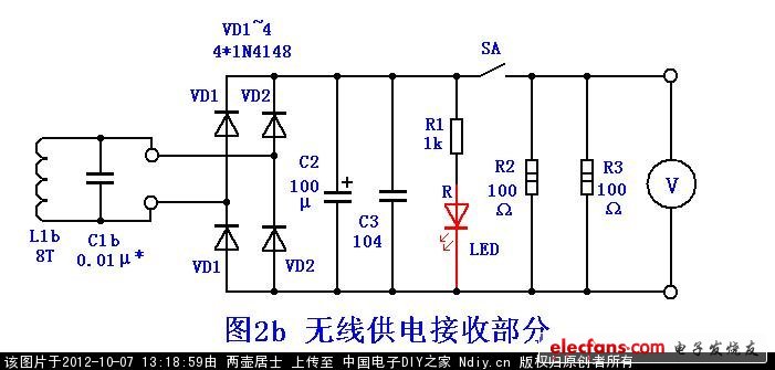
If the receiving distance and the conversion efficiency of the detection system are not tested, the circuit of Figure 2b may not be installed.
Part selection
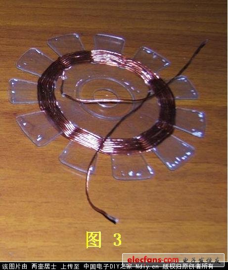
The efficiency of wireless power supply is related to the working state of the transmitting stage, and also has a very close relationship with the quality of the coil that emits electromagnetic energy. Therefore, the transmitting coil L1 uses 36&TImes; Φ0.1mm Litz wire, which is wound around the disc. Skeleton on the spider web. See Figure 3:
The skeleton of the coil is made of a disc, and in order to avoid eddy current loss, the metal plating on the disc should be removed. The inner diameter of the skeleton was 66 mm, and it was wound with a strand of 36 strands of Φ0.1. The receiving coil in Fig. 2b is also wound into a spider web, and is wound with 8 strands of Φ0.1 multi-strand enamelled wire.
The high-frequency output stage uses high-power FETs, such as the IRF series of 634, 630, or other VMOS tubes with a withstand voltage of 200V, a current of 5A, and a maximum loss power of more than 20W. Use a radiator with a large enough area when using it.
Resonant capacitor C4 requires a capacitor capacitor with a withstand voltage of 200V or higher; C11, C12, C13, and C14 require a withstand voltage of 35V or higher. Timing capacitors C5 and C10 require accurate capacitance and low leakage. It is best to use tantalum capacitors. If there is no tantalum capacitor, aluminum electrolysis with a withstand voltage of 25V or higher should be used. C7, C8, C11, and C12 should be soldered close to IC4.
There are no special requirements for other components.
Debugging and installation
First adjust the launch part. Input 24V DC power supply, when the debugging switch is in the off state, the red light of the LED will flash in about 1 second period, which indicates that IC2 is working normally. Close the debug switch SA in Figure 2a so that the oscillating portion operates continuously, and the red light will remain lit. Check whether the DC operating point of each point is normal. At this time, the current of the whole machine is about 50mA, and the drain current of VT3 is about 20mA. If the voltages at 24V and 9V are normal, the oscilloscope can be used to check the waveform of each key point.
When the waveform of each point is basically normal, use a 2200pF polyacrylic capacitor (withstand voltage of 250V) and a variable of 1000pF (multiple connected variable parallel connection), carefully adjust the variable to minimize the current of the whole machine. Measure the total capacitance in parallel, replace one or several fixed equivalent capacitors in parallel with the original fixed and variable capacitors, and solder them on the board.
Disconnect the maintenance switch SA to operate the oscillator in an intermittent state; rotate the Rp to the maximum to make the LED green light, gradually reduce the Rp, so that the green light of the LED is extinguished, and the red light just flashes. At this time, the whole machine current swings between 10 and 20 mA.
When the receiving portion is close to the transmitting coil and the load switch SA of the receiving portion is disconnected, the indicator LED on the receiver will flash in synchronization with the LED of the transmitting portion. Similarly, a fixed capacitor of about 0.01 μF is connected to both ends of the resonant coil, and the distance between the transmitting coil and the receiving coil is gradually opened, and the size of the resonant capacitor is appropriately increased or decreased to make the indicator light brightest. After adjustment, fix the capacitor and solder it on the board. If you observe the waveform of the resonant tank with an oscilloscope, you should see a sine wave with the same frequency as the transmitting coil.
Close the load switch SA (Fig. 2b) and place the receiving coil at 5~10mm directly above the transmitting coil. At this time, the green light of the two-color LED of the transmitting part will automatically light up, indicating that the transmitting part has detected the load and works. In a continuous state. If the receiving coil is removed again, the green light will automatically go out and the red light will flash again, indicating that the detection function of the smart part is normal. If the detection function is not normal, you should carefully adjust the Rp.
When the circuit detects the load, the total current of the transmitting part is about 200~300mA, which varies depending on the load.
Wireless power supply desk lamp
The circuit is basically the same as Figure 2b except that the 50Ω resistor as a dummy load is replaced by four high-power LEDs in series. The receiving coil is made of a disk-shaped coil with an enamel wire of Φ1.2 mm or thicker, and has an inner diameter of 67 mm around 8 turns, and a lead wire of 25 cm at each end, which will serve as a stand for the small table lamp in the future.
Find a disc, remove the metal coating, drill two holes in the appropriate place, thread the coiled leads through the holes in the disc, and bond the coil to the disc.
Mount 4 1W LEDs on a self-contained heat sink.
Also find a small disc with a diameter of 80mm (no need to remove the film) and a plastic bottle cap of appropriate size as the raw material for the lampshade for making the lamp.
The production process is shown in the series below.
summary
1. From the waveform of each point of the FET, the working state of the output stage is not very ideal, especially the high-order harmonics of the source voltage waveform, which obviously reduces the conversion efficiency of the circuit. The reason should be due to the excessive waveform of the gate drive voltage. If the gate waveform is changed to a narrower pulse, the conduction angle of the FET is made smaller, and the estimated efficiency is improved.
2. Due to the rush of production time, the 7809 analog voltage regulator circuit is directly used from 24V to 9V. The efficiency is obviously very low. If the switch regulator power supply is used, the efficiency of the drive part can be greatly improved, and the circuit can be operated intermittently. More power saving.
3. The device is designed to simulate a desktop wireless power supply system, so the distance between the transmitting coil and the receiving is greater than 12 mm, which also causes a significant drop in conversion efficiency, because the greater the distance between the two coils, the lower the efficiency.
4. The wireless desk lamp is only an application of wireless power supply, and the receiving part can also be used in the fields of wireless charging, underwater LED light or rotating LED graphic display.
5. Because the off-the-shelf wireless power supply module VOX330 is not easy to buy, the power supply uses 24V DC. If you have a high-voltage wireless power supply module at hand, it will be more practical to use 220V AC directly.
6 Layer PCB - stackup & prototype & price & manufacturing
What is 6 Layer PCB?
6 layer PCB Board is, in general, a 4 Layer PCB Board with 2 extra signal layers added between the planes. The 6-layer PCB classic stackup includes 4 routing layers (2 outer layers + 2 internal layers) and 2 internal planes (one for ground and the other for power). This enhances the EMI dramatically by offering 2 buried layers for high-speed signals and 2 surface layers for routing low-speed signals. The signal layers should be closed to the adjacent planes.
6 Layer PCB Prototype Fabrication China Manufacturer
Jinghongyi PCB has been committed to the production of multi-layer PCB and Prototype PCB for nearly 10 years. The largest number of multi-layer Printed Circuit Boards for customers are 4-layer, 6-layer, 8-layer, 10 layer, 12 Layer PCB and above. In order to ensure the quality of PCB products, we constantly improve and upgrade the production process. PCB surface treatment technology has hot air leveling(HASL), OSP, electroless nickel, immersion gold, immersion silver, immersion tin and so on.
The Printed Circuit Board is basically composed of the pad, via, solder mask layer, silkscreen layer, copper wire, and other parts. Among them, solder mask refers to the part covered by ink on PCB. Because most PCB uses green ink, the green ink part that can be seen is solder mask. The role of the solder mask in controlling the reflow welding process is very important. In addition to green ink, the welding layer can According to the different needs of customers, and can also be customized in a variety of colors, such as green, blue, black, red, white, yellow, purple. Of course, the price will vary with the color of the solder mask. Green oil is the one with low price and stable quality, which is also the reason why green oil is most used. The price of black oil, red oil, and white oil is almost the same, slightly more expensive than green oil, and the price of rare inks such as yellow and violet oil is the highest. In addition to the color of the solder resist ink, there are also matte and bright, matte ink color.
Based on our very experienced PCB engineer, we can help you in the 6-layer PCB stack up and design as much as possible.
In addition to providing you with 6-layer PCB and prototype manufacturing, we also provide one-stop prototype assembly services, including electronic components procurement, stencil, etc. The turnkey Printed Circuit Board Assembly services make your R&D work easy and time-saving.
6 Layer PCB Stackup and Design
What is PCB stack UP?
PCB Stack up refers to the arrangement of copper and insulation layers that make up PCB before the layout design of circuit board. Although stacking allows you to get more circuits on a single board through various PCB layers, the structure of PCB stacking design has many other advantages:- The PCB layer stack can help you minimize circuit noise and radiation and reduce impedance and crosstalk problems in high-speed PCB layouts.
- A good stacked PCB stack can also help you balance the need for low-cost, efficient manufacturing methods and focus on signal integrity issues.
- Proper PCB stacking can enhance the electromagnetic compatibility of your design.
- For PCB-based applications, stacked PCB configurations are usually good for you.
Why do PCBs stack up?
The irreversible development of modern electronic products has increasingly pushed PCB towards such needs as miniaturization, light weight, high speed, better functionality and reliability, and longer life, which has led to the popularity of multi-layer PCB. Two or more Single Sided PCB and/or Double Sided PCB are stacked together by a combination of semi-solid adhesives called "prepregs" to form multilayer PCBs through reliable predefined interconnections between them. There are three or more conductive layers in a Multilayer PCB , two of which are outside, and one is synthesized in an insulating board. With the increasing complexity and density of PCB, some problems may arise, such as noise.
One of the most important factors to determine the performance of product electromagnetic compatibility (EMC) is to plan the optimal multi-layer stack up. The carefully designed cascade can minimize radiation and prevent the circuit from being disturbed by external noise sources. Good stacked PCB substrates can also reduce signal crosstalk and impedance mismatch. However, poorer stacking may increase EMI radiation, because impedance mismatch will lead to reflection and ringing in the system, which will greatly reduce the performance and reliability of the product. Then, this article will focus on the layer stack definition, design rules and basic considerations.
Most six-layer PCB consist of four signal routing layers and two planes. From an EMC perspective, a 6-layer Printed circuit board is usually better than a 4 Layer PCB board.
6 Layer PCB Stackup

6 layer 1.6 MM standard stackup and thickness

Fig. 1 One of the stackup methods of 6-layer PCB
With six layers available the principle of providing two buried layers for high-speed signals is easily implemented as shown in Fig. 2. This configuration also provides two surface layers for routing low speed signals.

Fig. 2 Less common 6 layer PCB stackup
Not nearly as common, but a good performing stack-up for a six-layer PCB is shown in Fig. 2.

Fig. 3 Another performing six-layer PCB board stackup
Another excellent performing six-layer PCB board stackup is shown in Fig. 4. It provides two buried signal layers and adjacent power and ground planes and satisfies all five objectives. The big disadvantage, however, is that it only has two routing layers -- so it is not often used.

Fig. 4 Another excellent performing six-layer PCB board stackup

6 Layer PCB Stackup for EMI/EMC

EMI/EMC Return Current 6 Layer PCB Issue

EMI/EMC Return Current 6 Layer PCB Solved

Types of 6 PCB stack up-how to choose?
PCB materials and stackup thickness commonly used in multilayer circuit boards.
| 6 Layer Stackup - 0.8mm thickness | ||||||
| layer order | layer name | material type | material description | dielectric constant | thickness | copper weight |
| 1 | top | copper | signal | 0.035mm | 1 oz | |
| 2116 | prepreg | 4.5 | 0.12mm | |||
| 2 | inner 1 | copper | plane | 1 oz | ||
| core | 4.6 | 0.2mm | ||||
| 3 | inner 2 | copper | plane | 1 oz | ||
| 2116 | prepreg | 4.5 | 0.12mm | |||
| 4 | inner 3 | copper | plane | 1 oz | ||
| core | 4.6 | 0.2mm | ||||
| 5 | inner 4 | copper | plane | 1 oz | ||
| 2116 | prepreg | 4.2 | 0.12mm | |||
| 6 | bottom | copper | signal | 0.035mm | 1 oz | |
| Final board thickness: 0.8mm±0.1mm | ||||||
| 6 Layer Stackup - 1.0mm thickness | ||||||
| layer order | layer name | material type | material description | dielectric constant | thickness | copper weight |
| 1 | top | copper | signal | 0.035mm | 1 oz | |
| 2116 | prepreg | 4.5 | 0.12mm | |||
| 2 | inner 1 | copper | plane | 1 oz | ||
| core | 4.6 | 0.3mm | ||||
| 3 | inner 2 | copper | plane | 1 oz | ||
| 2116 | prepreg | 4.5 | 0.12mm | |||
| 4 | inner 3 | copper | plane | 1 oz | ||
| core | 4.6 | 0.3mm | ||||
| 5 | inner 4 | copper | plane | 1 oz | ||
| 2116 | prepreg | 4.2 | 0.12mm | |||
| 6 | bottom | copper | signal | 0.035mm | 1 oz | |
| Final board thickness: 1.0mm±0.1mm | ||||||
| 6 Layer Stackup - 1.6mm thickness (preferred materials) | ||||||
| layer order | layer name | material type | material description | dielectric constant | thickness | copper weight |
| 1 | top | copper | signal | 0.035mm | 1 oz | |
| 2116 | prepreg | 4.5 | 0.12mm | |||
| 2 | inner 1 | copper | plane | 1 oz | ||
| core | 4.6 | 0.6mm | ||||
| 3 | inner 2 | copper | plane | 1 oz | ||
| 2116 | prepreg | 4.5 | 0.12mm | |||
| 4 | inner 3 | copper | plane | 1 oz | ||
| core | 4.6 | 0.6mm | ||||
| 5 | inner 4 | copper | plane | 1 oz | ||
| 2116 | prepreg | 4.2 | 0.12mm | |||
| 6 | bottom | copper | signal | 0.035mm | 1 oz | |
| Final board thickness: 1.6mm±0.1mm | ||||||
| 6 Layer Stackup - 1.6mm thickness (non-preferred materials but possible) | ||||||
| layer order | layer name | material type | material description | dielectric constant | thickness | copper weight |
| 1 | top | copper | signal | 0.035mm | 1 oz | |
| 2116 | prepreg | 4.7 | 0.2mm | |||
| 2 | inner 1 | copper | plane | 1 oz | ||
| core | 4.6 | 0.5mm | ||||
| 3 | inner 2 | copper | plane | 1 oz | ||
| 2116 | prepreg | 4.5 | 0.12mm | |||
| 4 | inner 3 | copper | plane | 1 oz | ||
| core | 4.6 | 0.6mm | ||||
| 5 | inner 4 | copper | plane | 1 oz | ||
| 2116 | prepreg | 4.7 | 0.2mm | |||
| 6 | bottom | copper | signal | 0.035mm | 1 oz | |
| Final board thickness: 1.6mm±0.1mm | ||||||
| 6 Layer Stackup - 2.0mm thickness (preferred materials) | ||||||
| layer order | layer name | material type | material description | dielectric constant | thickness | copper weight |
| 1 | top | copper | signal | 0.035mm | 1 oz | |
| 7630 | prepreg | 4.7 | 0.2mm | |||
| 2 | inner 1 | copper | plane | 1 oz | ||
| core | 4.6 | 0.6mm | ||||
| 3 | inner 2 | copper | plane | 1 oz | ||
| 7630 | prepreg | 4.7 | 0.2mm | |||
| 4 | inner 3 | copper | plane | 1 oz | ||
| core | 4.6 | 0.6mm | ||||
| 5 | inner 4 | copper | plane | 1 oz | ||
| 7630 | prepreg | 4.7 | 0.2mm | |||
| 6 | bottom | copper | signal | 0.035mm | 1 oz | |
| Final board thickness: 2.0mm±0.2mm | ||||||
6
Layer Stackup - 2.0mm thickness (non-preferred materials but possible)
layer order
layer name
material type
material description
dielectric constant
thickness
copper weight
1
top
copper
signal
0.035mm
1 oz
2116+7628
prepreg
4.7+4.7
0.12mm+0.185mm
2
inner 1
copper
plane
1 oz
core
4.6
0.6mm
3
inner 2
copper
plane
1 oz
2116
prepreg
4.7
0.12mm
4
inner 3
copper
plane
1 oz
core
4.6
0.6mm
5
inner 4
copper
plane
1 oz
2116+7628
prepreg
4.7+4.7
0.12mm+0.185mm
6
bottom
copper
signal
0.035mm
1 oz
Final board
thickness: 2.0mm±0.2mm
6 Layer PCB Quote and Price
6 Layer PCB Prototype Price
Of course, at the same time, we also provide sample production services for other PCB products to verify your design as soon as possible.
With regard to delivery, we can provide 24-hour, 72-hour urgent service. No matter where you are in the world.
6 Layer PCB Manufacturing
- Manufacturable PCB Layers
We have abundant experience in manufacturing multi-layer circuit boards, not only in the production process, but also have many years of professional PCB engineers.So if you have multilayer PCB to produce, no matter how many layers, just let us know.
- What size of 6-layer circuit boards can you produce?
According to our PCB manufacturing capability, we have no size limitation.
- PCB Laminate Types
We offer a variety of PCB laminates ranging from FR4 130Tg for lower heating temperatures up to FR4 180Tg for higher temperatures. Also offered are Polyimide, Taconic, Rogers and Nelco material types.
- Manufacturable Thickness of 6-Layer Circuit Board
As with the number of PCB layers we can manufacture, we still have no restrictions on the thickness of the six-layer PCB and can manufacture it.
- PCB Surface Finish Types
We offer various PCB finishes including HASL (Solder), ENIG, Immersion Silver, Immersion Tin, Hard Gold, Entek/OSP, Unclad, Pb Free HASL, Selective Gold and ENEPIG.
Why order 6 layer PCB from JHY PCB?
You will get it after check below advantages.
1. Good quality and price: We are experienced in producing six layer PCB, cost and time can be controlled well. This can help our customer to order good boards in cost-effective price.
2. Short Turnaround Times:
3. No Minimum Quantity: 1 pcs of PCB can be offered.
4. More orders, more discount.
5. Custom PCB Sizes
6 Layer PCB
Printed Circuit Boards,6 Layer PCB,6 Layer PCB Price,6 Layer PCB Prototype
JingHongYi PCB (HK) Co., Limited , https://www.pcbjhy.com