In communication systems, students often face confusion when dealing with various protocols and interfaces, especially if they are new to the field. Different domains involve distinct types of communication and application designs, which makes it essential to organize and summarize key knowledge points effectively.
**The Origin of Level Standards**
During digital communication, signals are represented in high (1) and low (0) states. These correspond to specific analog voltage levels, which are determined by historical development and technological progress. For example, the early semiconductor devices were based on bipolar transistors, leading to the creation of TTL (Transistor-Transistor Logic). As technology advanced, particularly with the development of MOSFETs, CMOS (Complementary Metal-Oxide-Semiconductor) emerged, altering power supply requirements and changing the standards for digital output levels.
**TTL and CMOS Level Introduction**
TTL circuits typically operate at 5V. Their output levels are defined as:
- VOH > 2.4V (High)
- VOL < 0.4V (Low)
Input thresholds are:
- VIH > 2.0V (High)
- VIL < 0.8V (Low)
CMOS circuits can operate over a wider range, including 5V and 12V. Their output levels are:
- VOH > 4.99V (High)
- VOL < 0.01V (Low)
Input thresholds are:
- VIH > 3.5V (High)
- VIL < 1.5V (Low)
This shows that CMOS has a larger noise margin (1.5V) compared to TTL (0.4V).
**TTL and CMOS Gate Structures**
As shown in the diagrams, the TTL gate uses a push-pull output structure, with T4 functioning as an emitter follower. This results in low output resistance and strong load capacity.
In contrast, the CMOS gate uses complementary transistors, offering low power consumption and high noise immunity.
**Key Features of TTL and CMOS Drivers**
1. TTL has lower output resistance and stronger driving capability.
2. TTL operates in the nanosecond range, while CMOS is slightly slower but can match TTL speeds with advanced design.
3. TTL is current-driven, consuming more power and limiting large-scale integration.
4. CMOS inputs have higher impedance and are more susceptible to interference; they should not be left floating.
5. Modern IC technology combines both TTL and CMOS features in BiCMOS processes.
6. TTL and CMOS levels differ, requiring conversion for compatibility.
**Development of TTL and CMOS Levels**
TTL originally had a free interval between 2.4V and 5V. Later, low-voltage LVTTL was introduced, such as:
- 3.3V LVTTL: VOH > 2.4V, VOL < 0.4V
- 2.5V LVTTL: VOH > 2.0V, VOL < 0.2V
LVCMOS also evolved, with specifications like:
- 3.3V LVCMOS: VOH ≥ 3.2V, VOL ≤ 0.1V
- 2.5V LVCMOS: VOH ≥ 2.0V, VOL ≤ 0.1V
**High-Speed Level Standards**
To achieve high-speed operation, designers may increase drive current, lower voltage levels, or improve transistor speed. However, increasing current leads to higher power consumption, so adjusting level standards and improving transistor design is more practical.
**ECL and PECL Interfaces**
ECL (Emitter-Coupled Logic) and its variant PECL use differential structures and operate in the unsaturated region of transistors, significantly improving switching speed. They require a negative supply for ECL and positive for PECL. The output impedance is low, and the driving capability is strong.
**LVDS Interface**
LVDS (Low-Voltage Differential Signaling) uses low-voltage differential signaling for high-speed transmission. It offers low power consumption, strong noise immunity, and is widely used in high-speed applications.
**CML Interface**
CML (Current-Mode Logic) uses constant current drive and built-in termination resistors, making it ideal for short-distance, high-speed applications.
**Common Level Standards**
RS232 and RS485 are widely used in industrial applications. RS232 is a full-duplex interface, while RS485 is half-duplex and supports longer distances due to differential signaling. RS485 also provides better noise immunity and reliability.
**Protection Design and Connection Issues**
Interface protection is critical. Proper shielding, grounding, and circuit design help prevent damage from electrical surges or noise. Understanding how to connect DB9 connectors and manage signal lines is essential for successful implementation.
**Summary**
Digital level standards are fundamental in hardware design. While software protocols define communication methods, interface design remains a key challenge, especially in high-speed systems. Key areas to focus on include:
1. Understanding signal level application circuits.
2. Considering comprehensive protection and matching for different interfaces.
3. Following PCB design rules to minimize interference.
4. Conducting experiments to verify performance and solve real-world issues.
In conclusion, a solid theoretical foundation, careful design, and thorough testing are all essential for achieving reliable and efficient communication systems.
Frequency Inverter
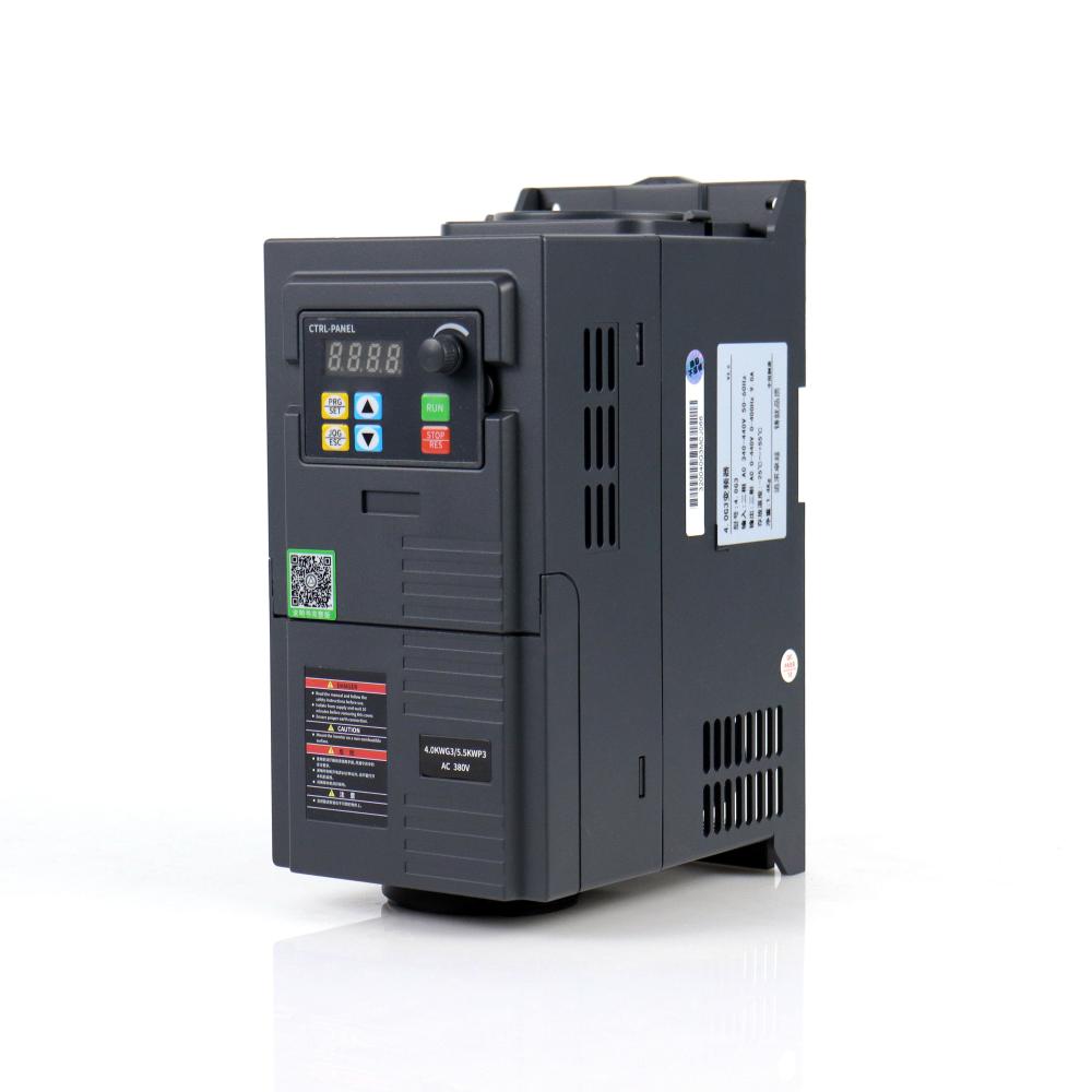
Frequency Inverters, also known as Variable Frequency Inverters or Variable Speed Drives, are electronic devices that are used to control the speed of an electric motor. They convert the incoming AC power into DC power and then back to AC power at the desired frequency and voltage. These devices are commonly used in industrial and commercial applications to regulate the speed of machines and equipment. Low Power Inverters, on the other hand, are designed for use in smaller applications such as home appliances and small machinery. They are typically less expensive and have a lower power output compared to their industrial counterparts. Overall, Frequency Inverters and Variable Frequency Inverters are essential components in modern industrial and commercial applications, while Low Power Inverters are more commonly used in smaller scale applications.
Frequency Inverter,Variable Frequency Inverter,Low Power Inverter,Variable Speed Drive

Frequency Inverter,Variable Frequency Inverter,Low Power Inverter,Variable Speed Drive
WuXi Spread Electrical Co.,LTD , https://www.vfdspread.com
