Op-amps are very high-gain amplifiers with differential inputs, single-ended outputs, and are often used in high-precision analog circuits, so their performance must be accurately measured. However, in an open-loop measurement, its open-loop gain may be as high as 107 or more, and pick-up, stray current, or Seebeck (thermocouple) effects may generate very small voltages at the input of the amplifier, and such errors will be difficult to avoid.
By using a servo loop, the measurement process can be greatly simplified, forcing the amplifier input to zero, allowing the amplifier under test to measure its own error. Figure 1 shows a multifunction circuit using this principle, which uses an auxiliary op amp as an integrator to create a stable loop with extremely high DC open-loop gain. The switch facilitates performing the various tests described below.
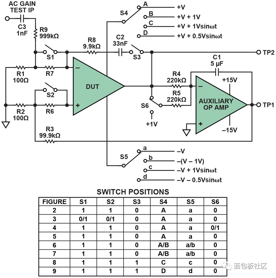
Figure 1. Basic operational amplifier measurement circuit
The circuit shown in Figure 1 minimizes most of the measurement errors and allows accurate measurement of large amounts of DC and a small amount of AC parameters. The additional "assist" op amp does not need to have better performance than the op amp to be tested, and its dc open-loop gain is preferably 106 or higher. If the offset voltage of the device under test (DUT) may exceed several mV, the auxiliary op amp should be powered from ±15 V (if the DUT's input offset voltage may exceed 10 mV, the resistance of the 99.9 kΩ resistor R3 needs to be reduced. )
The DUT's power supply voltages +V and –V are equal in amplitude and opposite in polarity. The total supply voltage is of course 2 × V. This circuit uses a symmetrical power supply, even for "single-supply" op amps, because the system ground is referenced to the intermediate voltage of the power supply.
The auxiliary amplifier as an integrator is configured for open loop (highest gain) at DC, but its input resistance and feedback capacitance limit its bandwidth to a few Hz. This means that the DC voltage at the output of the DUT is amplified with the highest gain by the auxiliary amplifier and applied to the non-inverting input of the DUT through a 1000:1 attenuator. Negative feedback drives the DUT output to ground potential.
(In fact, the actual voltage is the offset voltage of the auxiliary amplifier, more precisely the voltage drop caused by the offset voltage plus the bias current of the auxiliary amplifier due to the 100 kΩ resistance, but it is very close to ground, so it doesn't matter. Especially considering that the voltage change at this point during measurement is unlikely to exceed several mV).
The voltage at the test point TP1 is 1000 times the correction voltage (equal to the error in amplitude) applied to the input of the DUT, which is about tens of mV or more, so that the measurement can be performed with relative ease.
The offset voltage (Vos) of an ideal operational amplifier is 0, which means that when two inputs are connected together and the intermediate supply voltage is maintained, the output voltage is also the intermediate supply voltage. In reality, operational amplifiers have offset voltages ranging from a few microvolts to a few millivolts. Therefore, it is necessary to apply a voltage in this range to the input terminal so that the output is at an intermediate potential.
Figure 2 shows the configuration of the most basic test, offset voltage measurement. When the voltage on TP1 is 1000 times the DUT offset voltage, the DUT output voltage is at ground potential.

Figure 2. Offset voltage measurement
The ideal operational amplifier has an infinite input impedance and no current flows into its input. In reality, however, a small amount of “bias†current flows into the inverting and non-inverting inputs (Ib– and Ib+, respectively), which can cause significant offset voltages in high-impedance circuits. Depending on the type of op amp, this bias current may be a few fA (1 fA = 10–15 A, one electron every few microseconds) to several nA; in some ultrafast op amps, even 1 - 2 μA. Figure 3 shows how to measure these currents.
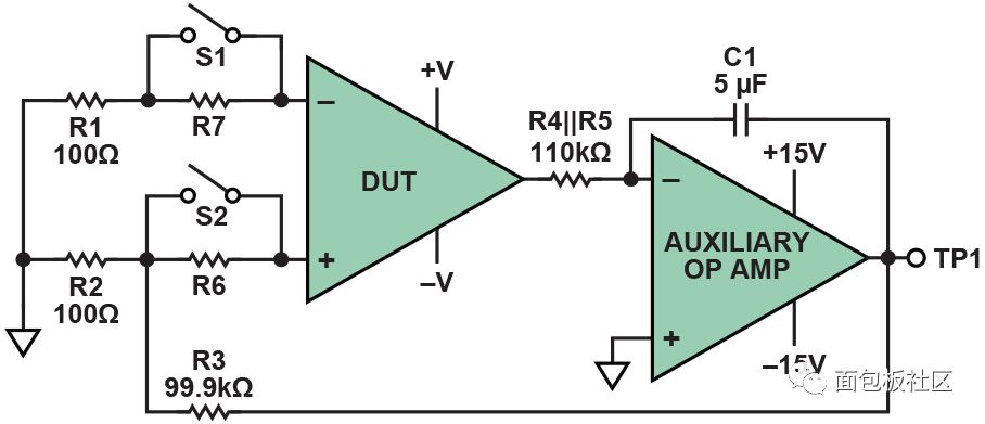
Figure 3. Offset and bias current measurements
This circuit is basically the same as the offset voltage circuit of Figure 2, except that the DUT inputs have two series resistors R6 and R7 added. These resistors can be short-circuited through switches S1 and S2. This circuit is identical to Figure 2 when both switches are closed. When S1 is off, the bias current at the inverting input flows into Rs and the voltage difference increases to the offset voltage. By measuring the voltage change of TP1 (=1000 Ib–×Rs), Ib– can be calculated. Likewise, Ib+ can be measured when S1 is closed and S2 is open. If the voltage of TP1 is measured first when both S1 and S2 are closed, and then the voltage of TP1 is measured again when both S1 and S2 are off, the “input offset current†Ios, ie, Ib+ and Ib– can be calculated by the change in the voltage. Difference. The resistance of R6 and R7 depends on the current to be measured.
If the value of Ib is around 5 pA, a large resistor will be used. Using this circuit will be very difficult and may require the use of other techniques involving the rate at which Ib charges the low leakage capacitance (used to replace Rs).
When S1 and S2 are closed, Ios will still flow into the 100 Ω resistor, causing Vos error, but it can usually be ignored in the calculation, unless Ios is large enough, and the resulting error is greater than 1% of the measured Vos.
The op amp's open-loop dc gain may be very high, and gains above 107 are not uncommon, but gains from 250,000 to 2,000,000 are more common. The DC gain is measured by switching R5 between the DUT output and the 1 V reference voltage through S6, forcing the output of the DUT to change by a certain amount (1 V in Figure 4), but if the device is powered by a sufficiently large power supply, it can be specified. 10 V). If R5 is at +1 V, the DUT output must be –1 V to keep the input of the auxiliary amplifier at zero.
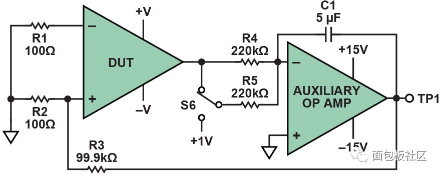
Figure 4. DC gain measurement
The TP1's voltage change is attenuated by 1000:1 and then input to the DUT, causing the output to change by 1 V, making it easy to calculate the gain (= 1000 × 1 V/TP1).
In order to measure the open loop AC gain, a small AC signal of the desired frequency needs to be injected at the input of the DUT and the corresponding output signal measured (TP2 in Figure 5). When completed, the auxiliary amplifier continues to maintain the average DC level at the DUT output.
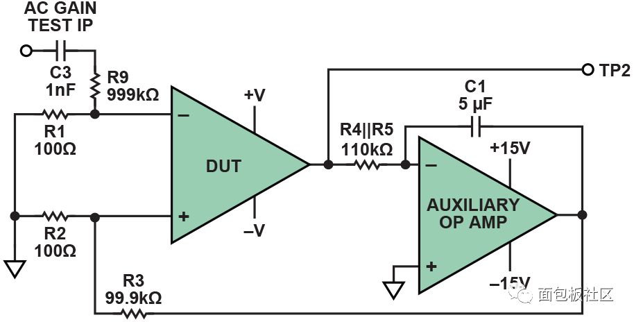
Figure 5. AC gain measurement
In Figure 5, the AC signal is applied to the DUT input through a 10,000:1 attenuator. For low-frequency measurements where the open-loop gain may be close to the DC value, such a large attenuation value must be used. (For example, at a gain of 1,000,000, a 1 V rms signal will apply 100 μV to the amplifier input, and an amplifier will attempt to provide a 100 Vrms output, causing the amplifier to saturate.) Therefore, the AC measurement frequency is typically a few hundred Hz to The frequency at which the open-loop gain falls to 1; when low-frequency gain data is required, measurements should be taken very carefully with a lower input amplitude. The simple attenuator shown can only operate at frequencies below 100 kHz. Even stray capacitances handled with care must not exceed this frequency. If more frequencies are involved, more complex circuits are needed.
The common-mode rejection ratio (CMRR) of an op amp is the ratio of the change in the offset voltage caused by a change in the common-mode voltage to the applied common-mode voltage change. At DC, it is typically between 80 dB and 120 dB but decreases at high frequencies. The test circuit is very suitable for measuring CMRR (Figure 6). Instead of applying a common-mode voltage to the input of the DUT to prevent the low-level effect from disrupting the measurement, the supply voltage is changed (in the same direction relative to the input, ie, the common-mode direction) and the rest of the circuit remains unchanged.

Figure 6. DC CMRR measurement
In the circuit shown in Figure 6, the offset voltage is measured at TP1, the supply voltage is ±V (+2.5 V and –2.5 V in this example), and the two supply voltages are again shifted up by +1 V (to +3.5 V and –1.5 V). The change in offset voltage corresponds to a 1 V common-mode voltage change, so DC CMRR is the ratio of offset voltage to 1 V.
The CMRR measures the change in offset voltage relative to the common-mode voltage and the total supply voltage remains the same. The power supply rejection ratio (PSRR) is the opposite. It refers to the ratio of the change in offset voltage to the change in total supply voltage. The common-mode voltage keeps the intermediate supply voltage constant (Figure 7).
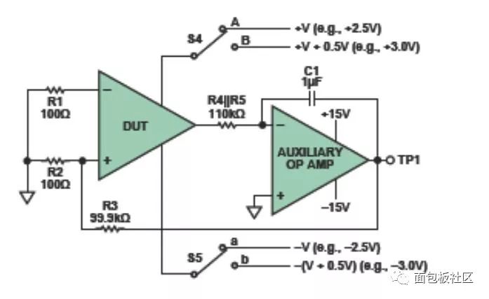
Figure 7. DC PSRR measurement
The circuit used is exactly the same, except that the total supply voltage changes while the common-mode level remains unchanged. In this example, the supply voltage is switched from +2.5 V and –2.5 V to +3 V and –3 V, and the total supply voltage is changed from 5 V to 6 V. The common-mode voltage still maintains the intermediate supply voltage. The calculation method is the same (1000 × TP1/1 V).
In order to measure AC CMRR and PSRR, it is necessary to modulate the supply voltage with voltage, as shown in Figure 8 and Figure 9. The DUT continues to operate under DC open loop, but the exact gain is determined by AC negative feedback (100 times in the figure).
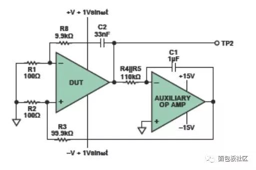
Figure 8. AC CMRR measurement
To measure AC CMRR, the positive and negative power supplies of the DUT are modulated with an AC voltage with a magnitude of 1 V peak. The modulation of the two power supplies is in phase, so the actual supply voltage is a stable dc voltage, but the common-mode voltage is a sine wave of 2V pp, causing the DUT output to include an ac voltage measured at TP2.
If the AC voltage of TP2 has an amplitude of x V peak (2x V peak-to-peak), the CMRR referred to the input of the DUT (that is, before the 100-fold AC gain is amplified) is x/100 V, and the CMRR is this value and 1 V peak The ratio. AC PSRR is measured by applying AC voltages to the positive and negative supplies that are 180° out of phase, thereby modulating the amplitude of the supply voltage (in this case, also 1 V peak, 2 V peak-to-peak), while the common-mode voltage remains stable. DC voltage. The calculation method is very similar to the calculation method of the previous parameter.
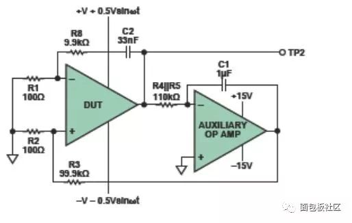
Figure 9. AC PSRR measurement
to sum up
Of course, there are many other parameters that opamps may need to measure, and there are many other ways to measure these parameters, but as shown here, the most basic DC and AC parameters can be easily constructed, easy to understand, and problem-free. Simple basic circuit for reliable measurement.
Wet Dry Vacuum Cleaner,Wet And Dry Vacuum Cleaner Price,Wet And Dry Vacuum Cleaner For Home,Wet And Dry Cordless Vacuum Cleaner
Ningbo ATAP Electric Appliance Co.,Ltd , https://www.atap-airfryer.com