The automotive environment is very demanding for electronics: any circuit connected to a 12V power supply must operate within the nominal voltage range of 9V to 16V. Other issues that need to be addressed urgently include load dump, cold start, battery Reverse, dual battery boost, spikes, noise and an extremely wide temperature range. When the load drops, the output voltage of the alternator rises rapidly to 60V or higher; cold start refers to starting the car at low temperature, which will cause the battery voltage to drop to 6V or lower; When a battery that is dead is activated, it is caused by carelessly connecting the polarity of the cable. Many tractors are equipped with two 12V batteries connected in series to help start a battery-powered car in cold weather. This will increase the voltage range of the electrical system to 28V until the car is started and the tractor driver disconnects the jumper cable.
This article refers to the address: http://
Considering that automotive electrical systems consist of high-current motors, relays, solenoids, lights, and constantly oscillating switch contacts, it's no surprise that spikes and noise are present. In addition, the alternator is a three-phase motor that is adjusted by chopper excitation, and sometimes charges the battery with a very large current. Therefore, for circuit designs operating in automotive environments, it is particularly desirable to accommodate high input voltage circuits that are generated with load dump and dual battery boost.
Passive protection circuit
The passive protection network for automotive electronics is shown in Figure 1. The same or similar circuits are widely used to protect various systems connected to the car's 12V bus. This network prevents damage from high voltage spikes, continuous overvoltages, battery reversal and excessive current consumption. The current protection effect of Figure 1 is obvious. If the load current exceeds 1A for a long time, the fuse F1 will melt. The combination of D1 and F1 prevents damage caused by reverse connection of the battery, and a large current flows through the forward biased D1 and blows the fuse. An interesting characteristic of an electrolytic capacitor is about 150% of the rated voltage: as the terminal voltage increases, this capacitor consumes more and more current. As far as C1 is concerned, it clamps as the input continues to rise. Function (final blow fuse). The voltage of the dual battery boost is about 28V, which does not blow the fuse, because the C1 25V rating is high enough and the additional current is very small. The inductor adds a small resistance to limit the peak fault current and the input transient's slew rate, helping C1 to clamp in the presence of spikes.
The main disadvantage of passive networks is that they rely on blown fuses to prevent damage from overcurrent, overvoltage and battery reversal. Another disadvantage is that it relies on electrolytic capacitors to achieve clamping. After the capacitor is aged, the electrolyte will dry out, and the characteristic of the equivalent series resistance (ESR) will disappear, which will damage the clamping effect. Sometimes D1 uses a large Zener diode to help this capacitor work. Active circuits have been designed to overcome these shortcomings.
Active circuit
Figure 2 shows an active solution for shielding sensitive circuits from the effects of variable 12V automotive systems. The LT1641 is used to drive the input N-channel MOSFET, and the passive solution described above does not have this additional protection: First, the LT1641 disconnects the load when the input is below 9V to prevent system failure at low input voltages, and Reduces the chance of the system providing valuable current to non-critical loads at start-up or when the charging system fails; secondly, the LT1641 gradually increases the output voltage during the first power-on, soft-starting the load; third, through current limiting and timing The circuit breaker protects the output from overload and short circuits. If a current fault occurs, the circuit breaker automatically re-attempts to establish a connection at a rate of 1 to 2 Hz. The tolerance of the protection circuit's upstream fuse can be set so that it does not melt when there is a current fault on the downstream line of the LT1641. Finally, Figure 2 The circuit isolation shown presents an overvoltage condition at the input and provides a clamp output so that the load circuit can continue to operate normally in the event of an overvoltage.
In the normal case of a 12V input, the LT1641 charges the gate of the MOSFET to approximately 20V to fully boost the MOSFET voltage and provide power to the load. Both ends of the 27V Zener diode D1 are connected to the gate and ground, respectively, but do not function in the operating voltage range of 9 to 16V. When the input rises above 16V, the LT1641 continues to charge the gate of the MOSFET in an attempt to keep the MOSFET fully turned on. If the input rises too high, the Zener diode clamps the gate of the MOSFET and limits the output voltage to approximately 24V. The LT1641 itself is capable of handling voltages up to 100V at its input and is unaffected by gate clamping. The gate clamp circuit is much more accurate than the clamp circuit of the passive solution, and the gate clamp circuit can be easily adjusted to meet the load requirements simply by selecting a D1 with a suitable breakdown voltage.
The circuit shown in Figure 2 works well at load currents up to about 1A, but for higher load currents, the circuit shown in Figure 3 is recommended to prevent excessive MOSFET power dissipation. If the overvoltage condition persists, such as when the electrical system is powered by two series-connected batteries for longer than the usual time, or if the current ramps up slowly after the load dips and the MOSFET is small, then excessive power consumption is risky. The output is sampled by D1 and D2. If the input exceeds 16.7V, a signal is fed back to the "SENSE" pin to stabilize the output at 16.7V. The adjustments here are more precise than the adjustments shown in Figure 1, and can be easily customized by selecting the appropriate Zener diode to meet the load requirements.
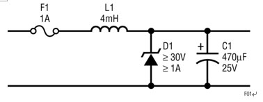
Figure 1: Passive protection network characterized by simplicity
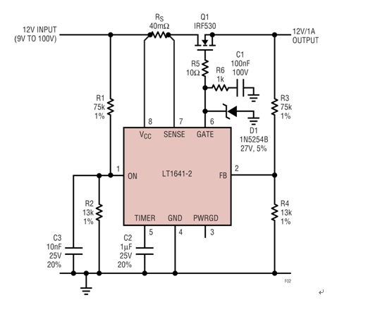
Figure 2: The overvoltage transient protector clamps the output at around 24V, and disconnects if the input drops below 9V.
The total power consumption is limited by the “TIMER†pin, which records the total length of time the MOSFET regulates the output. If the overvoltage condition persists for more than 15ms, the LT1641 shuts down and allows the MOSFET to stop output regulation. After about half a second, the circuit tries to restart. This restart period continues until the overvoltage condition disappears and resumes normal operation. The method of handling an overcurrent fault is the same as that described in FIG.
Battery reverse protection
By simply adding a series diode, you can add battery reverse protection to the circuit shown in Figure 2 or Figure 3.
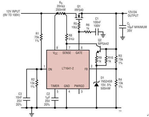
Figure 3: Adjusting the clamp voltage to clamp when the input surge rises, protecting the MOSFET from excessive power consumption
In most cases, a normal pn diode can be used. If the forward voltage drop is important, a Schottky diode can be selected. In a critical application where the power dissipation in the isolation diode is unacceptable, the simple circuit shown in Figure 4 can solve this problem.
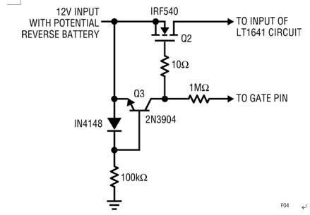
Figure 4: Battery reverse protection for Figures 2 and 3
Under normal operating conditions, the body diode of MOSFET Q2 is forward biased and delivers power to the LT1641. When the LT1641 is turned on, the Q2 gate is driven and fully turned on. If the input is reversed, the emitter of Q3 is pulled low below ground and Q3 is turned on, pulling Q2's gate low and keeping it close to the source level of Q2. In this case, Q2 remains off and isolates the inverting input from reaching the LT1641 and the load circuit. The microampere current flows through the 1MΩ resistor to the “GATE†pin of the LT1641.
High voltage LDO used as voltage limiter
Buck regulators with a maximum input voltage rating of 25V or less (such as the LT1616) are generally not considered for automotive applications. However, if combined with a low dropout (LDO) linear regulator such as the LT3012B/LT3013B, the disadvantages of the input voltage can be easily overcome. This small, high-efficiency combination, shown in Figure 5, provides a 3.3V output in an automotive environment.
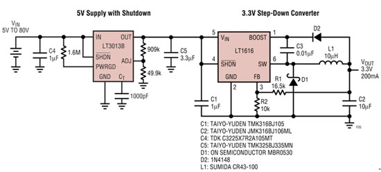
Figure 5: LT3013B used as a voltage limiter
With a wide input voltage range of 4V to 80V and integrated battery reverse protection, the LT3013B eliminates the need for special voltage limiting or clamping circuitry, saving cost and board space. When operating at moderate load currents, the efficiency of the LDO regulator is approximately equal to VOUT/VIN. If VOUT is much lower than VIN, the efficiency of the LDO will decrease. For example, when the 12V input is reduced to a 3.3V output, the efficiency is only 28%.
In Figure 5, higher efficiency is achieved by operating the LT3013B in a low dropout mode over the normal input voltage range. In this case, the output voltage of the LT3013B is set to 24V. The LDO's output voltage is only 400mV below VIN. It supplies the LT1616 buck regulator with 97% efficiency and the voltage is just in the middle of the normal operating voltage range. In the event of a load dump, VIN can quickly rise to as high as 80V, but at VIN over 24.4V, the LT3013B will adjust its output and effectively "limit" it to 24V, which is just within the rated voltage range of the LT1616 switch. Inside. If VIN rises above 24.4V, the efficiency of the LDO will decrease, but this situation is short and will not have any adverse consequences.
The LT1616 converts the LT3013B's limited output to 3.3V. At 12V input, the efficiency of the switch is approximately 80%. When the cold car is started, the voltage of the car may drop to 5V. In this case, the LT1616 has an input voltage of 4.6V, which is well within its operating voltage range. The LT3013B LDO regulator, combined with the LT1616 switch, provides a stable 3.3V output over a wide operating voltage range typical of 12V automotive electrical systems without sacrificing efficiency.
One more integrated solution is the LT3437. The LT3437 is a 200kHz monolithic buck regulator with an input voltage range of 3.3V to 80V. Its 100uA low quiescent current at no load is necessary to keep the system on and off today. A low cost diode can be placed in series with the input of the LT3437 to provide reverse battery protection.
Brushless DC Motor,DC Brushless Motor,24V DC Brushless Motor,High Torque Brushless Motor
Changzhou Sherry International Trading Co., Ltd. , https://www.sherry-motor.com