According to the editor, power electronic components are the general term for "passive" components. They are an important part of power electronic equipment, and they should be familiar to those who are engaged in the design, development, production, marketing and application of power electronic components and power supply technicians. This journal started to give lectures on "Power Electronics Component Knowledge" and the aforementioned "Power Electronics Device Knowledge" in April this year to meet the needs of the readers to increase their knowledge and make good use of these components. Engineers of manufacturers and users are welcome to write articles, and hope to put forward valuable comments.
Lectures on Power Electronic Components (5) New Inductors Mao Xingwu, Shandong Linyi Electronics Research Institute (Contributed) Zhang Naiguo (Adapted) of this journal (adapted) 1 Chip Inductor 1.1 Wire Wound Chip Inductor There are two types of power and high power.
(1) Low power wire wound chip inductors. The low-power wire-wound chip inductors are made of enameled wire wound on a ferrite or ceramic core (skeleton) with a smaller size. The shape and structure are as shown. Among them, the structure shown in (a) has a skeleton winding inside, and the outside is shielded by a magnetic material, which is formed by pressing a plastic film; (b) the structure shown is formed by winding a rectangular skeleton, and the skeleton has ferrite and ceramic Etc. (c) The structure shown is I-shaped, with ceramic, ferrite or aluminum as the skeleton, and the size is large.
(A) External plastic molding (with shielding); (b) Square ceramic or ferrite skeleton; (c) I-shaped ferrite skeleton chip inductor The main parameters are: size, inductance, allowable error, Q value , DC resistance, allowable maximum current and natural frequency (SRF). The operating frequency of the chip inductor mainly depends on the core material. In general, chip inductors with a skeleton material of ferrite are limited to work in the middle and low frequency bands, while chip inductors with a skeleton material of aluminum, ceramic or hollow can be used in high frequency bands, UHF (UHF) ) Section or VHF section. The inductance of the inductor suitable for the HF and UHF sections is generally 0.1 ~ 1000 | xH, and the inductance of the inductor suitable for the VHF section is generally 1.5 ~ 100nH. The tolerance of the inductance is usually level (+ 5%), K level ( ± 10%), M level (± 20%). The operating temperature range of chip inductors is generally -25 ~ 85. The disadvantage of small power wire wound chip inductors is that they are large and have large magnetic leakage. At present, most specifications of products have already been laminated chip. The inductor is replaced.
(2) High-power chip-wound inductors. In many circuits, surface-mount power inductors with an inductance of mH and current levels of A are required. High power wire wound chip inductors are mainly used as energy storage elements and LC filter elements in DC / DC converters. High-power chip-wound inductors are usually made of square or round I-shaped ferrite as the skeleton and enameled wires of different wire diameters, as shown.
Commonly used high-power chip-wound inductors have an inductance range of 1 ~ 330 | xH, and the inductance base has 1, 2.2, 3.3, 4.7, 5.6, 6.8, 8.2. 1.2 Multilayer chip inductors Multilayer chip inductors MLCI is a wire-free inductor made of ferrite material and using multi-layer production technology. Its structure is very similar to that of multi-layer chip capacitor (MLCC), as shown. Because the MLCI has a closed magnetic circuit, it has a shielding effect. The manufacturing methods of MLCI are divided into dry method and wet method. Among them, the dry method mainly refers to the cast-through method; the wet method includes the overlapping printing method, the via forming method and the printing hole forming method.
MLCI has the advantages of small size, high reliability, good magnetic shielding performance, and is suitable for high-density automatic placement of STM equipment. The inductance ranges from 1nH to several tens | xH. 1.3 Thin-film chip inductor Thin-film chip inductors are inductors made by using thin-film technology to engrave conductor coils on ceramics and other substrates, which can maintain high Q in the microwave section Value, high precision and high stability, and has a smaller size. Thin film chip inductors have a small parasitic capacitance, and the self-oscillation frequency of 1.4 chip integrated inductive elements (C) is suitable for surface assembly. It can be assembled on the PCB using standard chip mounter and reflow soldering technology. Conventional inductive components, such as choke and transformer, are generally non-standard lead forms and irregularly shaped devices, which require complex mounting equipment and manual assembly.
The wire frame is inserted into the slit, from side to side, and then bent into a standard "gull-wing" shaped lead. In this way, each lead wire in the lead frame becomes a half-turn winding of the inductor winding, and the other half-turn is composed of a lead on the PCB.
There are advantages in source system applications. C uses a high permeability and low loss core to expand the frequency characteristics, and can be used as a signal processing (SI-IC) pulse transformer or broadband transformer. The high-bandwidth, high-sensitivity iron core is suitable for EMC, such as common-mode chokes or double-line chokes that suppress power and signal line interference (EM-C). The chokes of different modes can be made with high permeability cores.
Chip inductors are mainly used in circuits such as filtering, resonance, oscillation, coupling, delay compensation, and impedance transformation.
Among the three passive components of resistors, capacitors and inductors, inductors are the most technically difficult and the most difficult to achieve chipping, and at the same time are the latest to achieve chipping. The rapid development of electronic whole machines towards light, thin, short and small has created a huge market for chip inductors. The application of chip inductors in the fields of computers, communications and audiovisual products is very large. Taking mobile phones as an example, each mobile phone is calculated by using 20 medium chip inductors. In 2007, the global mobile phone production was 1.144 billion units (of which China's mobile phone production is 549 million units), the use of chip inductors exceeds 22 billion. In addition to telephones and mobile phones, personal digital assistants (PDAs), digital cameras, portable CD players, VCDs, DVDs, video recorders, camcorders, color televisions, digital set-top boxes, fax machines, notebook computers, program-controlled switches, etc. are all required A large number of chip inductors.
When choosing a chip inductor, you need to consider the inductance, tolerance, frequency range, Q value, SRF, allowable maximum operating current, ==: knowledge lecture DC resistance and other parameters.
The quality factor Q value is an important parameter. It refers to the ratio of the inductive reactance of the inductor when it operates at an AC voltage of a certain frequency and the DC resistance of the coil (that is, Q = 2nfL / R). The smaller the inductor loss, the higher the Q value and the higher the efficiency. Q value is a parameter closely related to frequency. Inductors with high Q value at high frequency often have very low Q value at low frequency. Although different products have the same inductance, the DC resistance presented varies due to the different winding diameters selected. In the high-frequency loop, the DC resistance of the inductor has a great influence on the Q value, and care should be taken when designing.
2 Inductors based on amorphous and nanocrystalline alloy cores Amorphous and nanocrystalline alloy cores can be made into different shapes. The core used as an inductor is mainly ring-shaped. The conductor is wound on the ring-shaped iron core to make a number of turns, and it becomes an inductor. Shown is an amorphous nanocrystalline alloy ring inductor core and an inductor made from it.
Amorphous and nanocrystalline alloy inductors can be used in various power supply EMI filters, switching power supply output filters and power factor correction (PFC) circuits.
The switching power supply and the electromagnetic interference (EMI) filter circuit at the input end of the electronic ballast are as shown. In the figure, Li and A share a common core to form a common mode inductor. Li and L2 present high impedance to common-mode (asymmetric) interference signals, and low impedance to differential-mode interference signals (symmetrical interference currents) and power supplies. Very little.
The iron-based amorphous alloy core is suitable to replace silicon steel sheets and ferrites for the production of rectified power supply output filter inductors and reactors, intermediate frequency and high frequency (400Hz ~ 50kHz) switching power supply output filter inductors and audio equipment filter inductors. Shown is a switching power supply output rectification filter circuit using a forward converter topology.
In the figure, L is the filter inductor.
Filtering | Forward converter output rectification filter circuit adopts switching power supply, electronic ballast and frequency converter of bridge rectification capacitor filter circuit. Due to the existence of large-capacity smoothing filter capacitor, the rectifier diode is only at the peak of AC input line voltage It is turned on only nearby, so that the AC input current is no longer a sine wave, but a spike with a large amplitude. This severely distorted current waveform has a very low fundamental component and a very high harmonic content. As a result, the input power factor is very low (only about 0.55 to 0.60), and it causes pollution to the power grid and affects the connection to the same power network ( Safe and economical operation of other equipment in the system).
Using a power factor correction (PFC) circuit as shown, a sinusoidal current that maintains the same phase as the AC line voltage can be generated at the input of the bridge rectifier. The power factor can reach 0.99, and the total current harmonic distortion (THD) can be less than 10 % Or even 3%, and generates a boosted stable DC voltage (about 400V) at its output.
Among them, CiN and C. are PFC input and output capacitors respectively (CIN is used as high-frequency filtering, large-capacity electrolytic capacitors are not allowed), VT is PFC switch, IC is power factor controller, and L is boost inductor , VD is the boost diode. Circle or application
ZGAR FIT
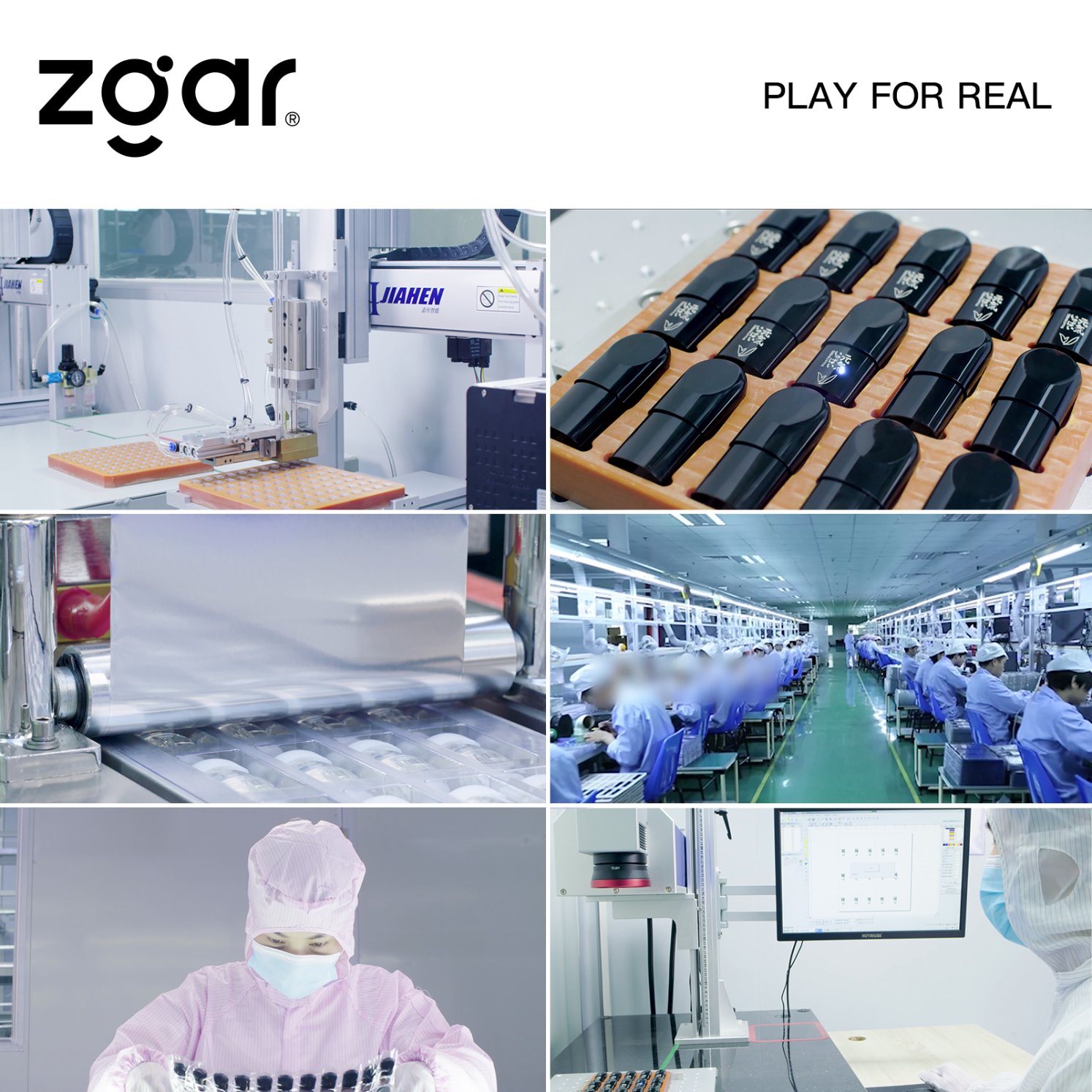
ZGAR electronic cigarette uses high-tech R&D, food grade disposable pod device and high-quality raw material. All package designs are Original IP. Our designer team is from Hong Kong. We have very high requirements for product quality, flavors taste and packaging design. The E-liquid is imported, materials are food grade, and assembly plant is medical-grade dust-free workshops.
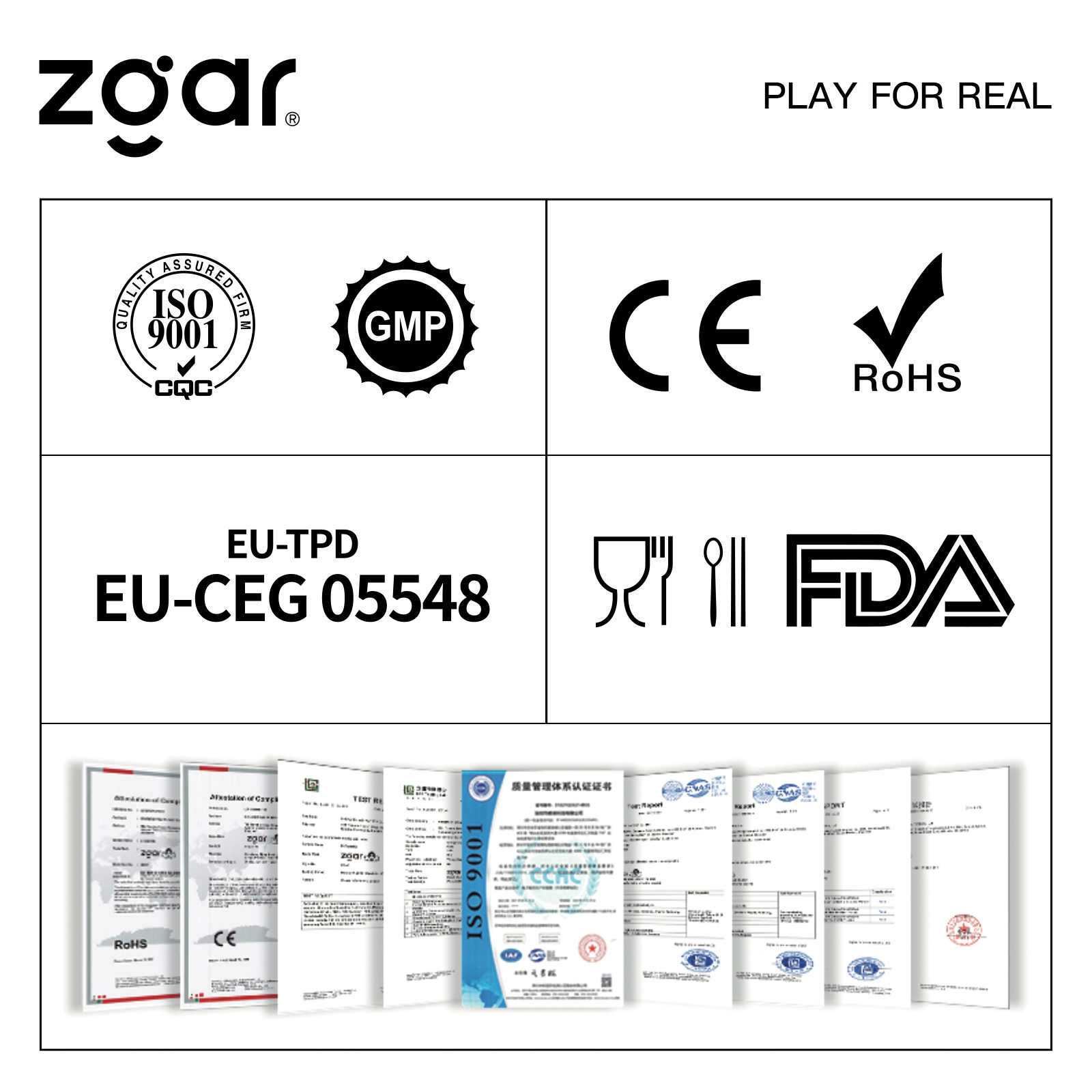
From production to packaging, the whole system of tracking, efficient and orderly process, achieving daily efficient output. We pay attention to the details of each process control. The first class dust-free production workshop has passed the GMP food and drug production standard certification, ensuring quality and safety. We choose the products with a traceability system, which can not only effectively track and trace all kinds of data, but also ensure good product quality.
We offer best price, high quality Vape Device, E-Cigarette Vape Pen, Disposable Device Vape,Vape Pen Atomizer, Electronic cigarette to all over the world.
Much Better Vaping Experience!


E-Cigarette Vape Pen,Disposable Device Vape,Vape Pen Atomizer,Latest Disposable E-Cigarette OEM vape pen,OEM electronic cigarette
ZGAR INTERNATIONAL TRADING CO., LTD. , https://www.sze-cigarette.com