The main circuit of the inverter is mainly composed of a rectifier circuit, a current limiting circuit, a filter circuit, a braking circuit, an inverter circuit and a detection sampling circuit. Figure 2.1 is its structural diagram. 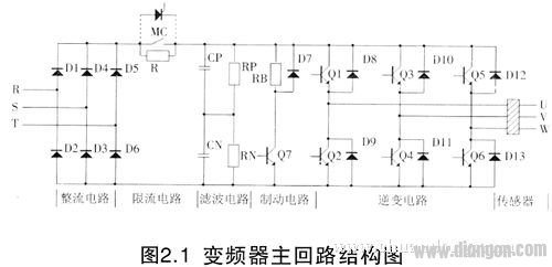
1) The driving circuit driving circuit is to provide the driving signals by the photoelectric conversion and amplification of the six PWM signals generated by the CPU in the main control circuit as the inverter circuit (inverter module).
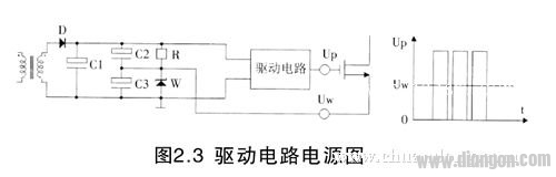
The various requirements for the drive circuit vary with the commutation device. At the same time, some developers have developed a number of dedicated drive modules for various commutation devices. Some brands and models of inverters use dedicated drive modules directly. However, most inverters use drive circuits. From a repair point of view, a more typical drive circuit is introduced here. Figure 2.2 shows the more common driver circuit (see Figure 2.3 for the driver circuit power supply). 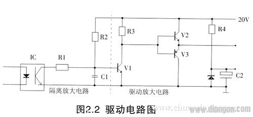
The driving circuit is composed of an isolation amplifying circuit, a driving amplifying circuit and a driving circuit power source. The three upper arm drive circuits are three independent drive power circuits, and the three lower arm drive circuits are a common drive power circuit.
2) Protection circuit When the inverter is abnormal, the loss caused by the abnormality of the inverter is minimized or even reduced to zero. Each brand of frequency converter pays great attention to the protection function, and tries to increase the protection function and improve the effectiveness of the protection function.
In the field of inverter protection functions, manufacturers can make a good example and make a good article. In this way, the diversity and complexity of the inverter protection circuit are formed. There are regular detection protection circuits and software integrated protection functions. Some inverter drive circuit modules, intelligent power modules, rectifier inverter combination modules, etc., have internal protection functions.
The circuit shown in Figure 2.4 is a typical overcurrent detection protection circuit. It consists of three parts: current sampling, signal isolation amplification, and signal amplification output. 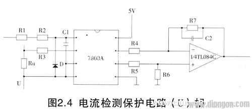
3) Switching power supply circuit The switching power supply circuit supplies low-voltage power to the operation panel, main control board, drive circuit and fan circuit. Figure 2.5 Structure of the Fuji G11 switching power supply circuit. 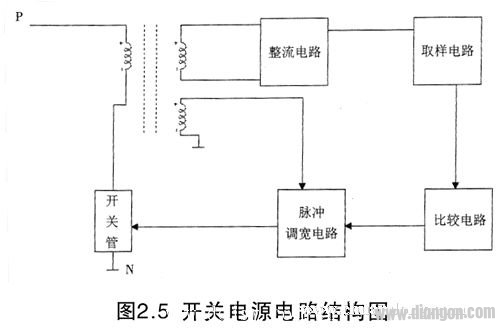
The DC high voltage P terminal is applied to the primary end of the high frequency pulse transformer, and the switch adjusting tube is connected in series with the other primary end of the pulse transformer, and then connected to the DC high voltage N terminal. The switch tube is periodically turned on and off to replace the primary DC voltage with a rectangular wave. The pulse transformer is coupled to the secondary, and after rectifying and filtering, the corresponding DC output voltage is obtained. It compares the output voltage to the pulse width adjustment circuit to change the pulse width to stabilize the output voltage.
4) Communication circuit on the main control board When the inverter is controlled by programmable (plc) or host computer, man-machine interface, etc., signals must be transmitted to each other through the communication interface. Figure 2.6 shows the communication interface circuit of the LG inverter. 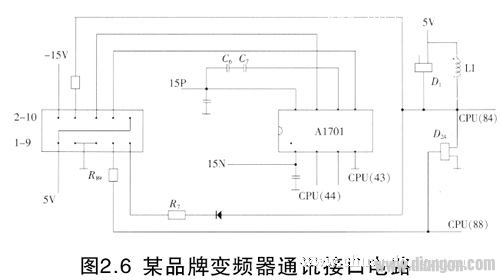
When the inverter communicates, the two-wire RS485 interface is usually used. The same is true for Siemens inverters. The two lines are used to transmit and receive signals, respectively. Before the inverter transmits the signal after receiving the signal, both signals pass through the integrated circuits such as buffers A1701 and 75176B to ensure good communication.
Therefore, the communication interface circuit on the main control board of the inverter mainly refers to this part of the circuit, as well as the anti-interference circuit of the signal.
5) External control circuit The external control circuit of the inverter mainly refers to frequency setting voltage input, frequency setting current input, forward rotation, reverse rotation, jog and stop operation control, and multiple speed control. The frequency setting voltage (current) input signal enters the CPU through the A/D conversion circuit in the inverter. Some other controls are passed to the CPU through optocoupler isolation of the input circuitry in the drive.
Gaming Headset,Gaming Headphones,Wireless Gaming Headset,Bluetooth Gaming Headset
SUNSHINE ELECTRONICS TECH. CO., LTD. , https://www.benefitucx.com