Wide Bandgap Semiconductor Gallium Nitride (GaN) and its related compound semiconductor materials are widely used in lighting and various optoelectronic components. Gallium nitride light-emitting diode (GaN LED) emits light from green to deep ultraviolet, and will completely replace traditional incandescent bulbs and fluorescent lamps as illumination sources for the foreseeable future.
Another potential optoelectronic component is the Micro Optoelectronic Device, which is a collection of thousands of emitters, detectors, optical switches (OpTIcal Switches) or optical waveguides (OpTIcal). Micro-components such as Waveguide) are on a single wafer. ITRI ​​expects that the future of micro-optical array components will play an important role in the fields of display, biosensor, optical communication or optical fiber communication, optical interconnect (Interconnect) and signal processing (Signal Process).
Micro LED Array uses the addressable driving technology as a display. In addition to LED's high efficiency, high brightness, high reliability and fast response time, its self-illuminating display - no backlight required The characteristics are more energy-saving, simple in mechanism, small in size and thin. Compared with organic light-emitting diode (OLED) displays, which are also self-illuminating, Micro LEDs have better material stability, long life, no image imprinting, etc. Their unique high brightness characteristics are used in projection display applications such as micro Projection (Pico ProjecTIon), head-mounted optical display (See-through HMD), head-up display (HUD), etc., are more competitive. In addition, the high-speed response of the Nano Second level makes the LED display more suitable for high-definition (3D) display, high-speed modulation and transmission of signals, as a visible light wireless communication function of smart displays.
Micro LED technology
The wafer surface of a Micro LED microdisplay must be fabricated in an array structure like an LED display, and each Pixel must be addressable and individually driven to illuminate. If driven by a complementary metal-oxide-semiconductor (CMOS) circuit, it is an active addressing drive architecture, and the micro-LED array chip and the CMOS can be electrically connected by a package technology such as Flip Chip Bonding. After the bonding is completed, the Micro LED can improve brightness and contrast by integrating a Microlens Array. Figure 1 shows a passively addressed Micro LED microdisplay chip. The Micro LED array connects the positive and negative poles of each Micro LED through a vertically interleaved positive and negative grid electrode (P-metal Line & N-metal Line). The power is sequentially applied, and the Micro LED is illuminated by scanning to display an image. Actively driven displays are more energy efficient and faster than passive matrix drives, and have always been the mainstream driver for high resolution displays.

Figure 1 Micro LED passive addressing array architecture and wafer photo
Micro LED technology challenges need to be broken
Micro LEDs ("50 micrometers (μm)) have different characteristics than ordinary size ("100 micron") LEDs. For example, general-sized LEDs have almost no problems such as current crowding (Current Crowding), thermal stacking, etc., and may have better efficiency due to lattice stress release and larger light-emitting surfaces. In contrast, a large surface area of ​​a Micro LED may have a large leakage path due to a large number of surface defects, and a micro electrode may increase the series resistance value, which may affect the luminous efficiency. Therefore, the development of micro LED array process and the structural design of micro LEDs must overcome the above problems. In addition, the uniformity of Micro LEDs is related to imaging quality and product yield, which is one of the technical development challenges.
In fact, the current Micro LED microdisplays are single-color, because it is difficult to simultaneously epitaxially grow different wavelengths on a single substrate, and maintain high-quality LEDs. Therefore, according to the literature, the US 3M may convert blue (or UV) light into red, (blue) and green light through the quantum well photoexcitation layer in a wavelength conversion manner to form a chromophoric (RGB) pixel. Sony (Sony), OKI and other manufacturers tend to use the technology of transferring red, blue and green Micro LED epitaxial films (Epi-film Transfer) to form a color micro LED array. At the scale of Micro LED pixels of about 10 microns, RGB array technology is a technical bottleneck that every team in the world needs to break through.
Progress in technology research and development in various countries
At the end of 2011, Professor Jiang's team at Texas Tech University published the world's most densely populated (1,693dpi) green-light active-addressed Micro LED array chip (Figure 2), which is a video graphics array (VGA). ) (640 & TImes; 480) resolution. The microdisplay combines a Micro LED array and a CMOS drive integrated circuit (IC). Each Micro LED unit has a drive transistor circuit that can individually control the illumination.

Figure 2 Active addressing micro-grain LED array microdisplay developed by Texas University of Science and Technology
By optimizing lithography and etching in semiconductor processes (Figure 3), Ostendo Technology of the United States achieved a uniformity of 98% and a density of up to 2,450 dpi on a 4 å‹ LED wafer. The development of this technology has contributed to the practical application of high resolution LED microdisplays. Ostendo will also use this technology to make a laser diode (LD) array as a projection display source, which will have better optical efficiency than LED microdisplays in projection applications.
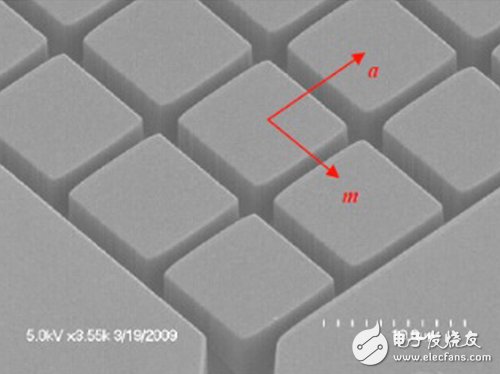
Figure 3 Ostendo Technology develops process technology for micro LED array with a pitch of 10μm
Professor Dawson of the University of Strathclyde in the United Kingdom has invested heavily in the research of Micro LED. Figure 4 shows a 64×64 microdisplay made by it. They integrated microlens integrated circuits onto the Micro LED array to increase display brightness. In 2010, the research team in China also established mLED company to provide Micro LED technology platform to cooperate with customers to develop related application modules or products such as medical, micro display, printing, semiconductor process light source.

Figure 4 64×64 Micro LED array developed by mLED
Figure 5 shows a 240×160 Micro LED component manufactured by the Institute of Electro-Electrical Engineering. The component size is 7.4 mm (mm) x 4.9 mm and the micro LED pixel pitch is 30 microns (846 dpi). The Institute of Electro-Optical Engineering has produced red, blue and green micro-LED arrays and developed them in a single wafer for integrated red, blue and green-light micro-LEDs to realize single-chip Micro LED full-color display chips.

Figure 5 Image of 240×160 blue LED micro-array array component fabricated by ITRI
Dongguan Yuantong Technology Co., Ltd. is a professional production of each block cutting machine, flat mouth machine, folding machine, express bag machine, Pearl Cotton Bag Cutting Machine, slicing machine, degradation bag cutting machine, all kinds of plastic bag mold, punching machine, electrosick machine and other supporting equipment, and according to the special requirements of customers design and production of special equipment.
Express bag making machine, bag making machine,Express bag all-in-one machine
Dongguan Yuantong Technology Co., Ltd. , https://www.ytbagmachine.com