Ultra-wideband (UWB) low noise amplifiers are widely used in intermediate frequency and video amplification systems. These circuits not only amplify video signals but also handle a wide range of pulse and RF signals, from DC to several megahertz or even tens of megahertz. As a result, they are extensively applied in signal processing. In recent years, UWB technology has seen rapid development in areas such as secure communication and target detection. With increasing bandwidth demands, the front-end receiving circuit must be capable of handling ultra-wideband signals efficiently. Therefore, a low-noise, ultra-wideband amplifier is essential. The CMOS-based low noise amplifier designed in this paper operates within a frequency range of 3 to 5 GHz and is specifically tailored for UWB applications. The paper begins with the selection of the LNA structure and then proceeds to analyze and design the ultra-wideband LNA configuration.
In traditional broadband LNA designs, distributed and balanced amplifier techniques are commonly used. However, these approaches often require significant DC power consumption to achieve better broadband performance and input matching, making them unsuitable for UWB systems. Recently, alternative structures such as band-pass filter input matching and parallel resistance negative feedback have been introduced in UWB LNA designs. The former offers a large bandwidth, flat gain, and good noise performance, but requires a higher-order bandpass filter to extend the frequency range. The latter expands the bandwidth by introducing a resistive feedback loop that reduces the input quality factor. By incorporating noise cancellation techniques, the noise figure can be further optimized. Figure 1 shows the schematic diagram of the circuit structure used.
In Figure 1, the main amplifying section of the circuit uses a parallel negative feedback Cascode structure. C1, C2, and C3 are on-chip DC blocking capacitors, while Rf is the feedback resistor and Cf is a DC blocking capacitor on the feedback loop. Lg and L1 are part of the input matching network for narrowband LNAs. M1 is a common-source transistor, acting as the main amplification device, and its noise figure and input matching are critical to the overall performance. M2 is a common-gate transistor, which provides greater reverse isolation and helps suppress the Miller effect of M1. L2, Rd, and Cd form a low-Q load to extend the output bandwidth. M3 and M4 together form a source follower for the output stage. Together, M1, M2, M3, and M4 create a feedforward noise cancellation structure. The bias circuit is omitted in the diagram, but Vbias_1 and Vbias_2 represent the bias voltages.
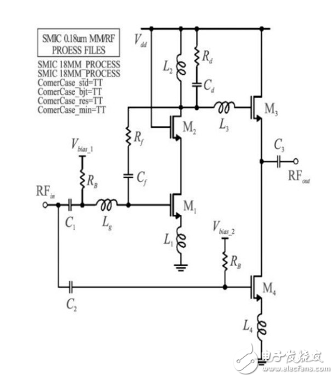
**Figure 1: Schematic diagram of low noise amplifier circuit structure**
**Circuit Analysis and Design**
**Broadband Input Matching Analysis**
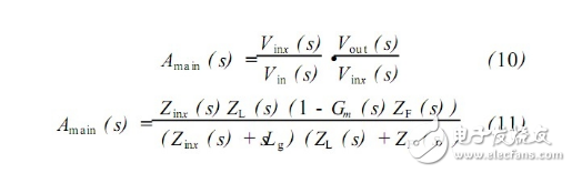
In Figure 1, the output buffer M3 is removed. The inductively degraded structure formed by M1, M2, and L1 converts the input voltage into an output current, effectively functioning as a transconductance stage with a transconductance of Gm. This allows us to derive the small-signal equivalent circuit of the main amplifying section, as shown in Figure 2. The value of Gm is typically found in literature, and here M2 is treated as an ideal current transmitter, ignoring secondary effects to obtain meaningful results.
In Figure 2, Cgs1 represents the gate-source capacitance of M1, Z4(s) is the input impedance of the M4 feedforward loop, and L2, Rd, and Cd form the load impedance. Gm1 is the transconductance of M1. For the impedance analysis at point X in Figure 2, we find:
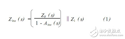
**Figure 2: Core circuit small signal equivalent circuit diagram**
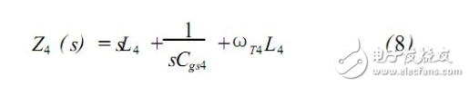
The input impedance of the M4 feedforward loop can be expressed as:
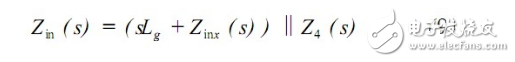
Therefore, the input impedance expression of the LNA becomes:
Due to the complexity of equation (9), numerical analysis using MATLAB is performed instead of symbolic derivation. Under the given simulation conditions and feasible circuit parameters, the results shown in Figure 3 are obtained. It can be observed that within the 3 to 5 GHz range, the real part of Zin is very close to 50 Ω, and the imaginary part is near zero at approximately 4.2 GHz. The magnitude of Zin remains close to 50 Ω, indicating successful broadband input matching. The transistor sizes and values of Lg and L1 are provided: M1 = M2 = 320 μm / 0.18 μm, Lg = 2.6 nH, and L1 = 0.32 nH.
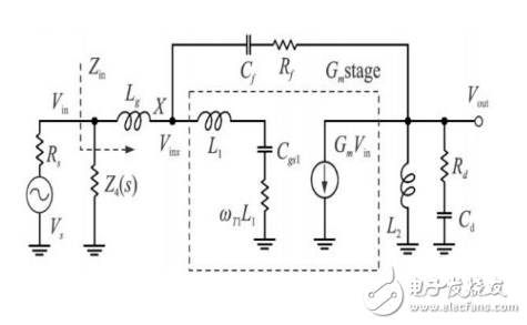
**Figure 3: Zin's MATLAB simulation results**
**Gain Analysis**
By analyzing and deriving the circuit in Figure 2, the gain Amain(s) of the main amplifying circuit can be expressed as:
Where Zinx(s) is the impedance to ground at point X. To increase the circuit gain, the equivalent transconductance Gm and the load impedance ZL can be increased. However, these parameters are frequency-dependent, and their changes can affect the gain flatness, requiring careful trade-offs during the design process.
To further enhance the gain of the main amplifier, an inductor L3 is connected in series with the gate of the output buffer M3. The gain boosting mechanism can be explained using the amplifier equivalent model shown in Figure 4(a). CLoad represents the input capacitance of M3. Figure 4(b) shows the small-signal equivalent circuit of the model. The gains derived from the small-signal equivalent circuits are:
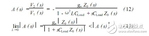
From equations (12) and (13), it is clear that the introduction of inductor L3 increases the gain. When L and CLoad resonate at ω2, the following relationship holds:
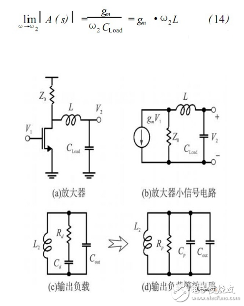
**Figure 4**
In wideband LNAs, the output load must be a low-Q circuit to maintain broad bandwidth performance.
48V Lithium Battery,lithium battery bicycle,Electric Bicycle Battery,lithium electric bicycle
Shenzhen Jentc Technology Co., LTD , https://www.phenyee.com